


Commercial powders made of two copper oxides were compacted with spark plasma sintering (SPS). Their dielectric properties were studied in a broad range of frequencies and temperatures. Various relaxation phenomena were documented. DC resistivity was measured as well. Microstructure and phase composition were studied, and phase purity was shown for CuO, whereas Cu2O was more sensitive to carbon contamination during the SPS processing. Influence of the sintering temperature on microstructure and electrical properties was described for both materials. Change of DC resistivity induced by visible light irradiation was monitored for 48h. The overall difference between CuO and Cu2O from the electrical standpoint was finally not so dramatic as the stoichiometry indicated. Both materials exhibited giant permittivity, but extremely dependent on frequency and temperature. Application could find such systems mainly in the branch of sensors.
Se compactaron polvos comerciales compuestos por dos óxidos de cobre mediante sinterización por plasma por chispa (SPS). Se estudiaron sus propiedades dieléctricas en una amplia gama de frecuencias y temperaturas. Se documentaron diversos fenómenos de relajación. También se midió la resistividad mediante métodos de corriente continua. Se estudiaron la microestructura y la composición de las fases, y se demostró la pureza de la fase para el óxido cúprico (CuO), mientras que el óxido cuproso (Cu2O) fue más sensible a la contaminación por carbono durante el procesamiento del SPS. Se describió la influencia de la temperatura de sinterización sobre la microestructura y las propiedades eléctricas de ambos materiales. Se monitorizó el cambio de la resistividad de campo eléctrico directo inducido por la irradiación de luz visible durante 48 horas. La diferencia general entre CuO y Cu2O desde el punto de vista eléctrico finalmente no fue tan dramática como indicaba la estequiometría.
Due to their abundance in the earth's crust, cuprous oxide (Cu2O) and cupric oxide (CuO) are gaining increased attention as promising materials for optoelectronic applications. They exhibit the most important criteria of the future: availability, sustainability, nontoxicity, and ease of synthesis [1]. These metal oxides show superior charge carrier mobility and display higher environmental stability as compared to other solution-processed semiconductors such as organic polymers and small molecules. Cu2O and CuO are hole conducting p-type oxides by virtue of their cation vacancies [2].
The charge carrier mobility of CuO (about 0.1cm2/Vs) is much lower than that of Cu2O, which has higher hole mobility (of about 100cm2/Vs) and more pronounced p-type character due to the presence of a higher number of copper vacancies [2–4]. However, both Cu2O and CuO are non-stoichiometric oxides with copper vacancies, Cu2−δO and Cu1−yO, respectively, and both are p-type semiconductors [5].
Heating in air leads to oxidation of Cu2O to CuO rather easily. The oxidation rate of Cu2O forming CuO after the complete consumption of copper (if Cu metal is the starting composition of the studied material) at 600–1000°C is slow. The activation energy for the Cu2O oxidation is relatively high at 600–800°C but becomes very low or eventually negative at an even higher temperature [6].
Cu2O forms a cubic structure in the Pn3m space group with a lattice parameter of 0.427nm, whereas CuO exhibits a square planar coordination of copper with oxygen in the monoclinic structure. The lattice parameters of CuO are a=0.4684nm, b=0.3425nm, c=0.5129nm and angle β=99.28° [3].
Applications of CuO could be found in a selective solar absorber since it has high solar absorbency and low thermal emittance. Furthermore, it is a promising semiconductor for solar cell fabrication [3]. Its application of photoelectrochemical splitting of water was also studied [3]. The second material, Cu2O, is suitable also as photo-absorber in the industrial applications, mainly in the form of thin films [4]. The role of both copper oxides lies in possible replacement of other compounds with similar behaviour, that contain elements like Ga, Se, In. In contrast to them, in the case of copper oxides their abundance, sustainability, nontoxicity of the elements, and rather non-expensive production via many processes was mentioned as an important advantage [1].
Among these processes, sintering has a central role in production of bulky parts. Most powder materials undergo sintering at temperatures well above one half of their melting point. In the case of copper oxides, the sintering temperature is rather low, markedly below 1000°C, and this fact contributes to rather good economical balance of the process. The driving force of sintering is the excessive surface free energy available in the materials. There are several ways to enhance sintering either by altering the process kinetics, or the driving force. Their general trend is to reduce the sintering time or sintering temperature without compromising the degree of densification. Most of the conventional techniques of consolidation result in significant growth of the grain structure. This way, the desired benefits of fine-grained structure on material properties are not obtained. To circumvent this factor, the non-conventional consolidation methods utilize high sintering speed and short sintering time. The resulting lowered temperature induces improvements in mechanical properties of the products due to the limited grain growth [6]. Between these techniques, spark plasma sintering (SPS) has a prominent position. The co-sintering of Cu2O with ZnO, to form a heterojunction, was described in Ref. [7]. The SPS parameters were 800°C (reached within 8min), 100MPa and 6min dwell time.
The reasons why to study copper oxides are two-fold. They attracted certain attention as functional materials. The second serious reason is that they are oxidation products of copper, one of the key metals in the electrical industry. To know their physical behaviour in electric field is therefore an important task. The goal of this paper is to sinter CuO and Cu2O via SPS and obtain the dependence of dielectric parameters on the sintering temperature. The motivation is to find an optimum sintering way for these materials in the SPS process and, on the other hand, to study general background of the electrical behaviour of these materials in the SPS-processed form. Based on powders available on the market, we compared CuO and Cu2O having a rather dissimilar size distribution.
ExperimentalPowders and sinteringPowder CuO was purchased from Alfa Aesar (Karlsruhe, Germany); Product 33307, with 99% purity. Powder Cu2O was also purchased from Alfa Aesar; Product 40188, with 99% purity. This second one was described by the producer as −200mesh (i.e., under 74μm).
Cylindrical discs of about a 3mm height and a 20mm diameter were sintered by SPS 10-4 system (Thermal Technology, USA) using graphite die and punches at temperatures between 700°C and 850°C (reached within 8min), applying in all cases a pressure of 100MPa and a dwell time of 8min. Optimization of the SPS parameters was done in a broader range, 600–1000°C, 70–120MPa, 3–10min. The final values were selected mainly based on the criteria of a crack-free character of the sample.
Characterization techniquesPhase analysis was done by XRD. The powder X-ray diffraction (PXRD) measurements were carried out on a vertical θ–θ diffractometer D8 Discover (Bruker AXS, Germany) using CuKα radiation. The diffracted beam was detected by 1D detector LynxEye and the signal was recorded in the angular range 15–120° 2θ. Quantitative Rietveld refinement was performed in the TOPAS V5 software using fundamental parameters approach for evaluation of lattice parameters, average sizes of coherently scattering domains and micro-strain.
The surface of specimens was made smooth by grinding to eliminate surface roughness and possible superficial contamination from the carbon foils used at SPS. Scanning electron microscopy (SEM) observation was performed using Phenom-Pro microscope (Thermo Fisher Sci., Eindhoven, The Netherlands) equipped by CeB6 thermionic cathode and working in the backscattered electron (BSE) mode. All images were collected at 15kV electron beam voltage.
Open porosity was determined with Archimedean (water immersion) technique.
Layers of aluminium as thin film electrodes were sputtered on both sides of each sample. A three-electrode measurement fixture was used to measure dielectric parameters of the samples. The electric field was applied parallel to the SPS pressure direction.
Capacitance at room temperature was recorded in the frequency range from 20Hz to 1MHz using a programmable impedance analyser model 4284A (Agilent, USA). Applied voltage was 1V AC. Relative permittivity ɛr calculation was based on the measured capacitance CP and specimen dimensions. The same arrangement and equipment were used also for the loss tangent measurement at the same frequencies as capacitance.
Capacitance, loss tangent as well as AC resistance were measured also at elevated temperatures up to 150°C. Measurements at elevated temperatures were carried out using a Novotherm heating unit 2108 (Novocontrol, Germany) equipped with a special broadband dielectric spectroscopy (BDS1200) sample fixture.
Electric resistance, and also its evolution in time, were examined with a special resistivity adapter – Keithley model 6105. The DC electric field was applied from a regulated high-voltage source and the values were read by a multi-purpose electrometer (617C, Keithley Instruments, USA). Magnitude of the applied voltage was 100±0.05V. Volume resistivity calculation was based on the measured resistance and specimen dimensions.
Run of the DC resistance in combination with illumination were continuously monitored for 48h. The illumination was done using the conventional bulb with a hot tungsten filament inside. Its spectrum is contiguous from 0.4 to 2.5μm, with maximum intensity at about 1.1μm. The electrical power of 60W was applied. To complete a full cycle, the light was switched on after each 3h and switched off again after next 3h, repeatedly, until the end of experiment.
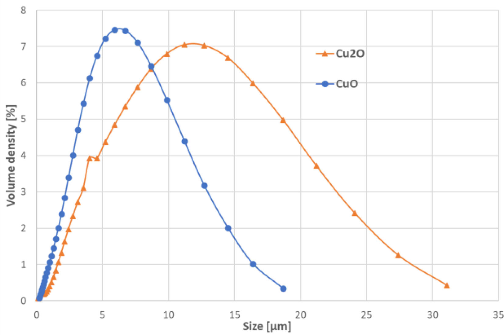
ResultsPowder size distributionThe powder size distribution, measured by laser granulometry (Malvern Analytical, England), was for the CuO powder given by the volume density Dv(10)=1.63μm, Dv(50)=5.41μm, and Dv(90)=11.50μm. Concerning Cu2O, the volume density parameters were: Dv(10)=2.55μm, Dv(50)=9.17μm, and Dv(90)=20.10μm. The whole distribution, expressed in volume density, is displayed in Fig. 1.

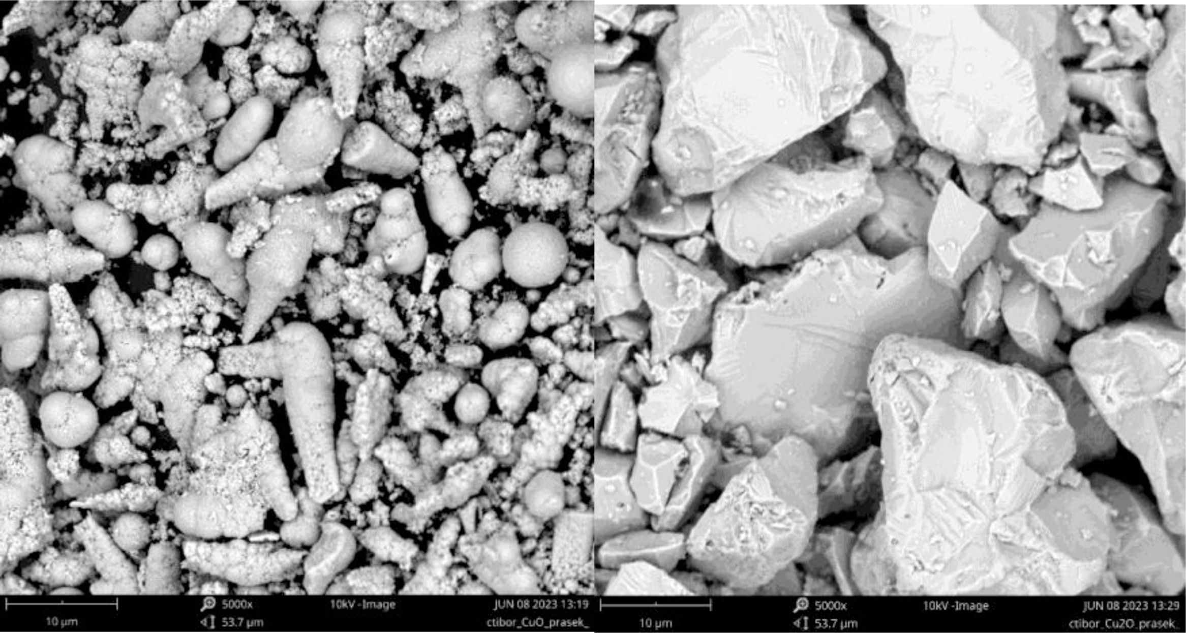
The difference between the used powders was too complicated to be adequately described only be numbers associated with size quantification. The values were also influenced by the presence of ultrafine particles, as visible in Fig. 2. Particularly in the case of CuO, they were numerous. The character of the CuO powder was nodular with nearly spherical or variously elongated particles, each of them composed also from grains of a size reaching either sub-micrometric, or a few micron size. It looked like agglomerated-and-sintered nano-powder. In contrast, the Cu2O powder was facetted, blocky and evidently coarser. The appearance was like for a fused-and-crushed product. Such powder would need more thermal energy for the same sintering level. Coarser particles result in a smaller contact area, compromising the reactivity during sintering and, consequently, disfavouring the densification of the sintered bodies.
SPS parameters and Cu2O, scale bars 10μm.")
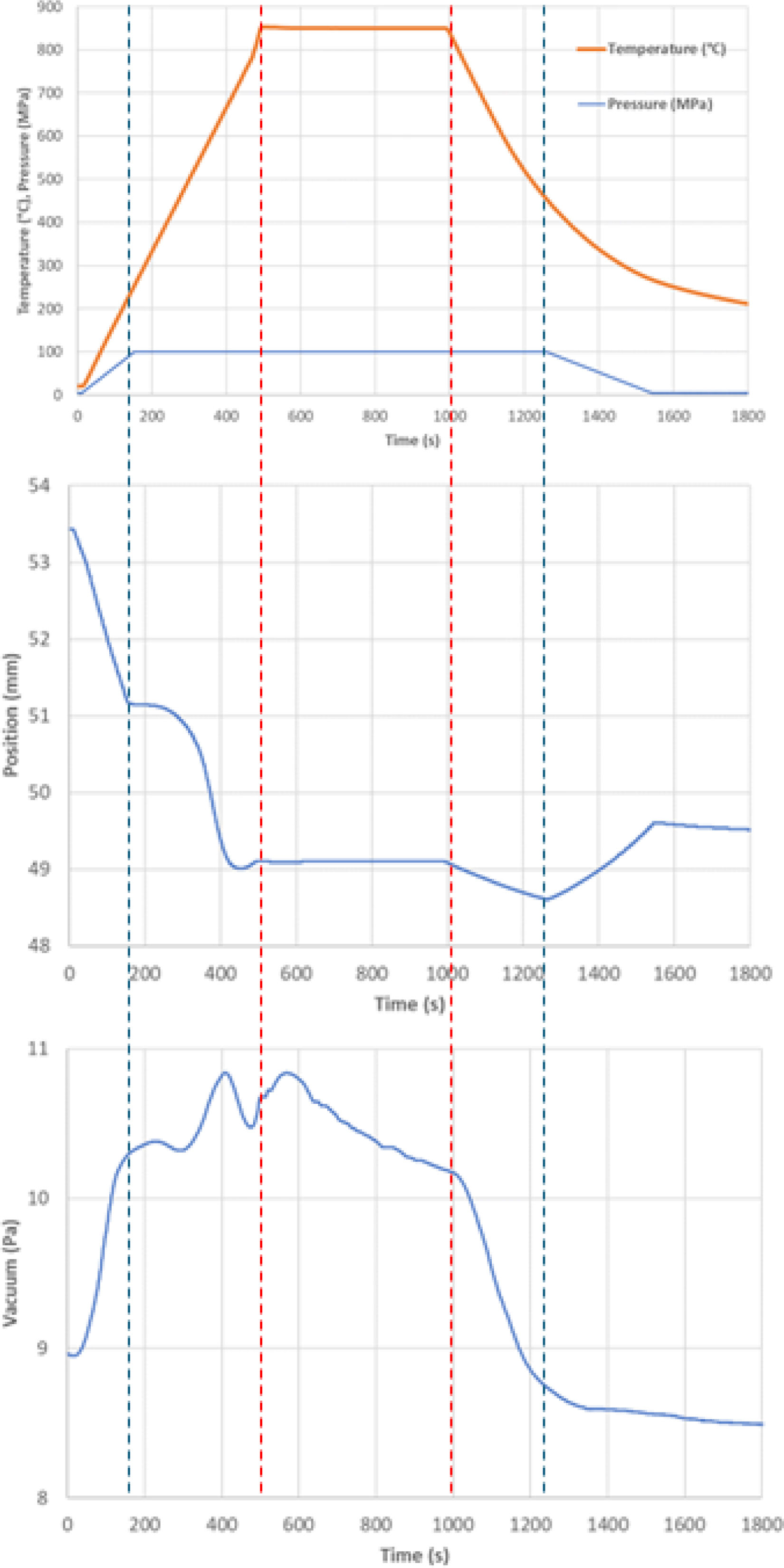
The evolution of the main SPS sintering parameters is schematically displayed in Fig. 3. The uniaxial pressure of 100MPa was achieved at the moment of reaching the temperature 250°C. The pressure in the chamber decreased (i.e., vacuum up) during heating. When the temperature reached about 670°C, the vacuum level worsened again because of the air released from the gaps between particles at this temperature. The punch position, Fig. 3, was initially changing during heating, up to about 670°C, which was caused by the initial movement of the particles in the powder. During and after the dwell time at the maximum temperature, the punch position was nearly constant. This is a sign of proper compaction conditions. The cooling ramp is not actively controlled, and the actual rate is comparable to air quenching (from 800°C to 200°C it needed 800s, which represent quenching rate 45°C/min; however the temperature monitoring under 400°C is not very reliable).

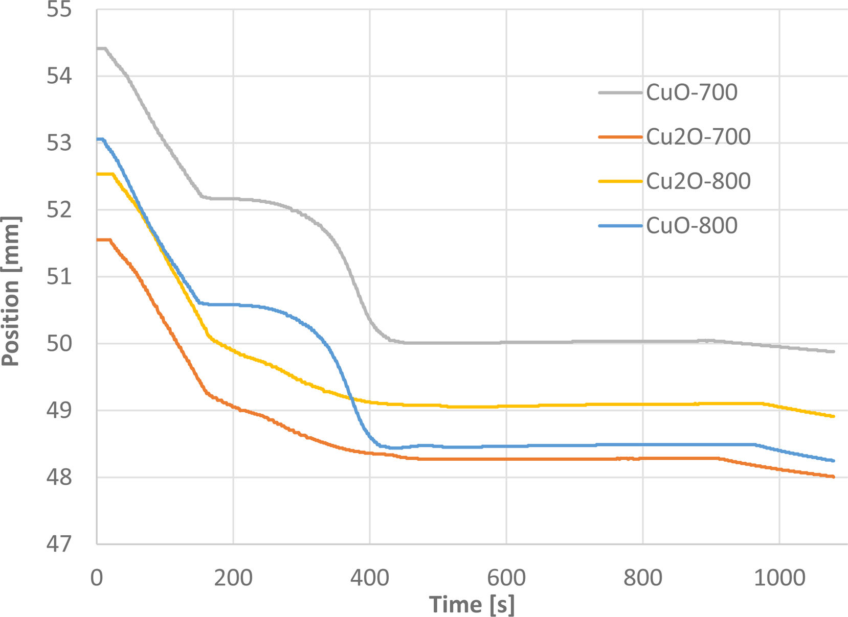
Fig. 4 shows the piston shift versus the SPS processing time. For Cu2O, it was rather contiguous, whereas for CuO, there was a stagnation period followed with a fast compression of the powder. The interval, where the two copper oxides differ, was between 180 and 400s, corresponding roughly to the temperature between 300°C and 670°C. Cu2O particle size (volume density d50=9.17μm) of the initial powder was nearly two times larger than that of the CuO powder (volume density d50=5.41μm). The finer particles of CuO resisted better to the pressure, and therefore the run of the compression was slowed in a certain temperature range where the powders were completely solid and rigid, without plasticization.
Microstructures
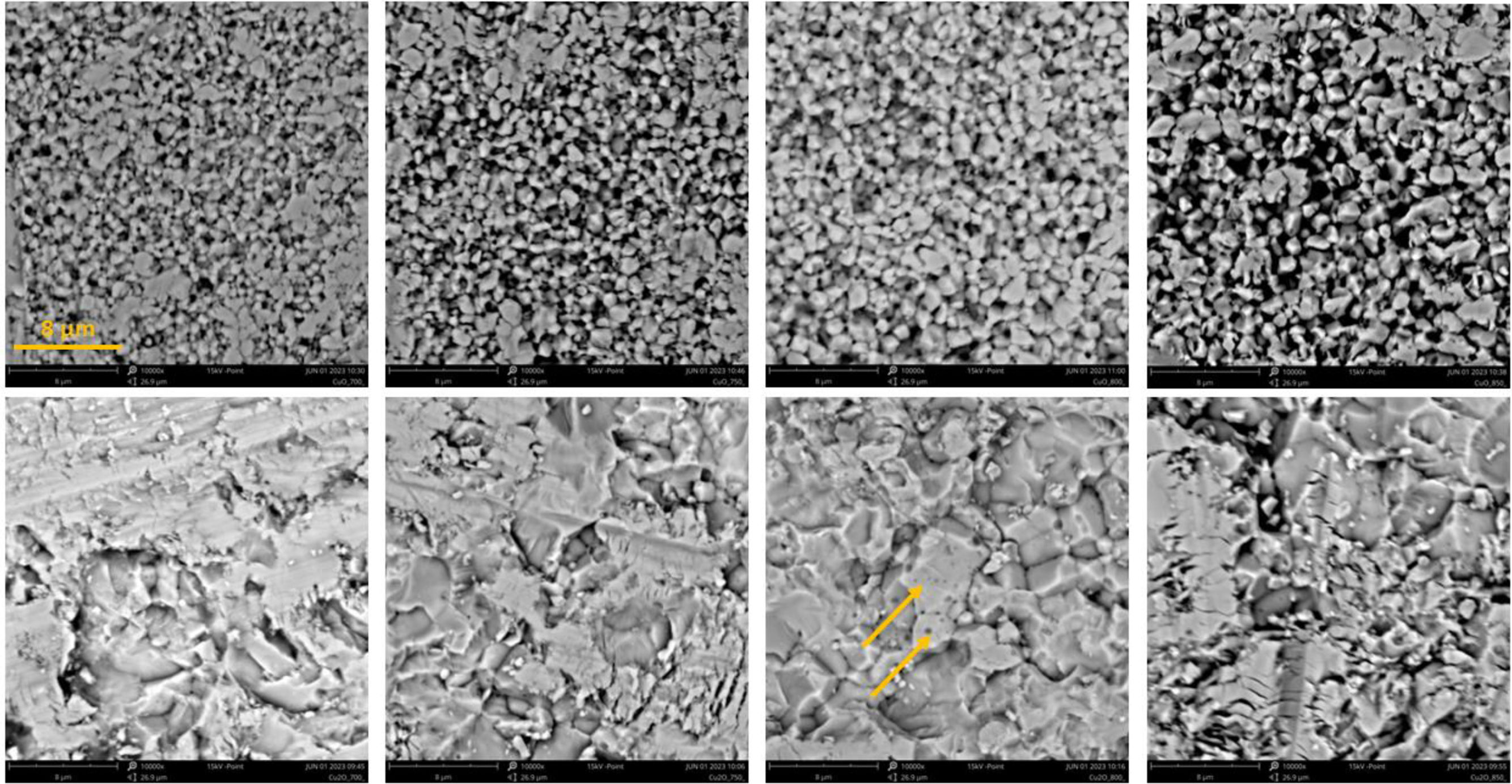
The micrographs, Fig. 5, represent the sample surface after grinding and slight polishing, which represents its preparation “under an electrode” for the dielectric measurement. So, this was not a “free surface”, and not a “polished section”, but an intermediate state, a surface after removal certain layer of the material (about 0.2mm) by SiC paper of a #280 grade. We have used this approach for various materials to simulate conditions of surface treatment relevant for industry, where “metallographic polishing” of ceramics is never applied “under an electrode” for many technological and practical reasons. Such images are, however, unsuitable for porosity determination via image analysis. Concerning CuO, the samples looked like sintered, but with less intimate contact between the neighbouring particles, leading to porosity origin. Pores were present, and even the less porously appearing sample CuO-800 showed rather separated grains. The grain size was relatively homogeneous with an average diameter estimated around 1μm. In the case of Cu2O, the grains were coarser, but more compact microstructure, without frequent pores, was observed. The samples of Cu2O (after the same surface treatment) looked more deformed, and the microstructure was partly heterogeneous with a (less easily estimated) grain size of about 10μm. In the case of the Cu2O-800 sample, globular pores inside large grains were present, indicated with arrows. Practically no grain coarsening was seen for both materials, considering the initial powder size.
X-ray diffraction results
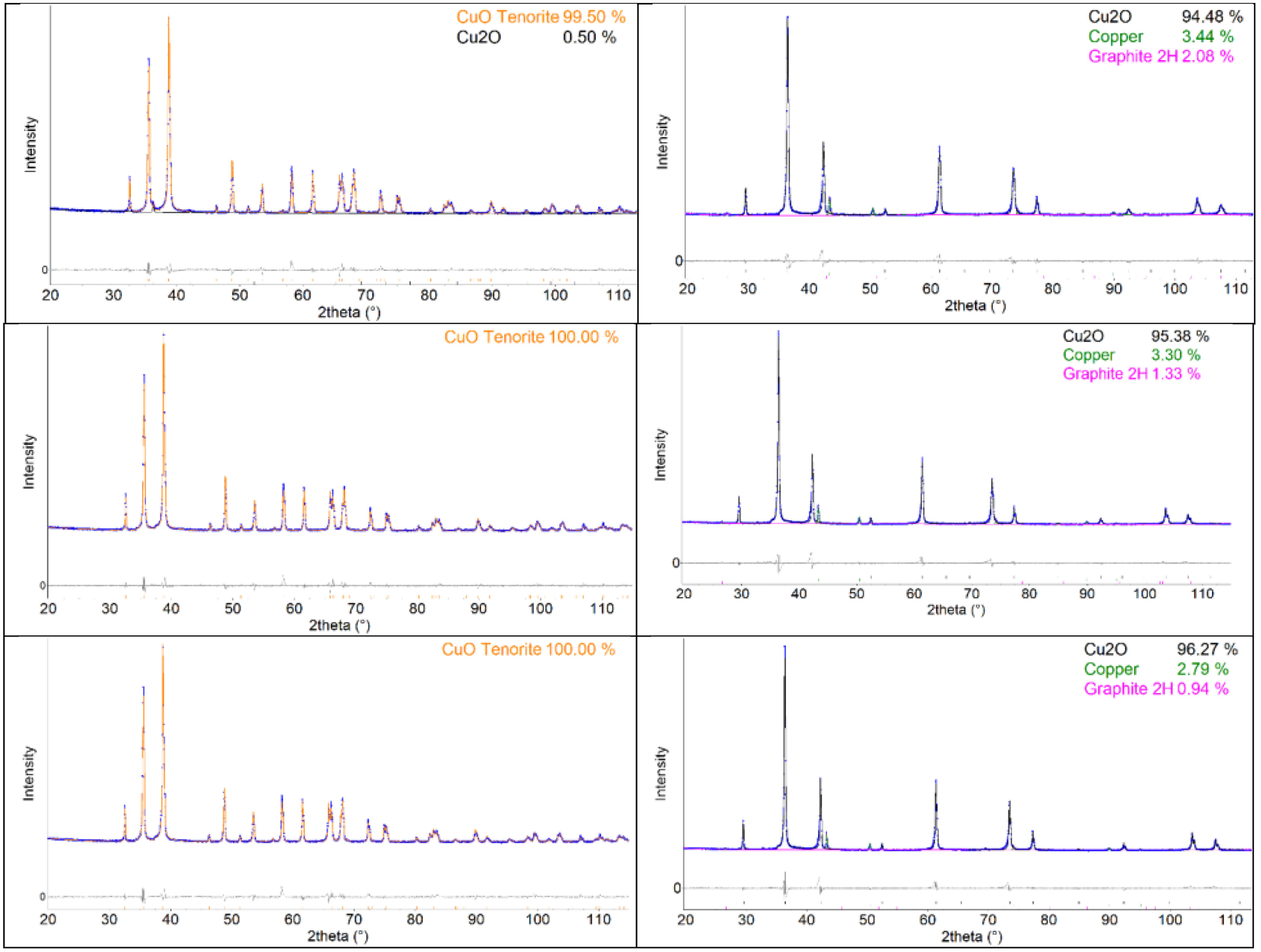
The phase composition showed purely the CuO tenorite phase for the CuO powder, Table 1, whereas for Cu2O powder, besides 97.3% of Cu2O cuprite, also 2.7% of CuO was detected, Table 2. This indicated probably Cu2O powder production by reducing CuO, which was not fully finished. During SPS processing, CuO was nearly fully phase-pure, whereas Cu2O was prone to certain chemical reduction (Fig. 6).

Table 2 shows the phase composition of the material, nominally being Cu2O. From 2.8% to 3.3% of metallic Cu was detected. The second undesired phenomenon was contamination with graphite from the SPS apparatus – C content of 0.9% to 2.1% (Table 3).
The Cu2O crystallite size was, expectedly, monotonously increasing with the sintering temperature for Cu2O, Table 3. For CuO, the difference between 750 and 800 samples is negligible. The growth was faster, whereas in the case of Cu2O, part of the thermal energy was consumed for other phenomena, especially reduction and carbonization. The higher the temperature, the better the phase purity of the Cu2O sample (c.f. Table 2).
The dislocation density calculated for our SPS samples is in Table 4, using the measured crystallite size and the recalculation as mentioned in the literature [4]. The results for our SPS samples are close to the literature, where it was 2.26×10¹⁴lines per m2[4] for a Cu2O thin film, or elsewhere 6.40×10¹⁴lines per m2[8] for CuO synthesized using the hydrothermal method.
The density, based on water-immersion measurements, is shown in Table 5. For CuO, the trend was a slight decrease of density with the sintering temperature. For Cu2O, due to impurities in the sample and phase separation, c.f. Table 2, the comparison between samples would be irrelevant. At 800°C, the Cu2O sample was denser than CuO sample.
In the work on Cu–Cu2O composites sintered by SPS [9], the density of Cu2O is listed as 6.14g/cm3, but our sample Cu2O-800 was not pore-free.
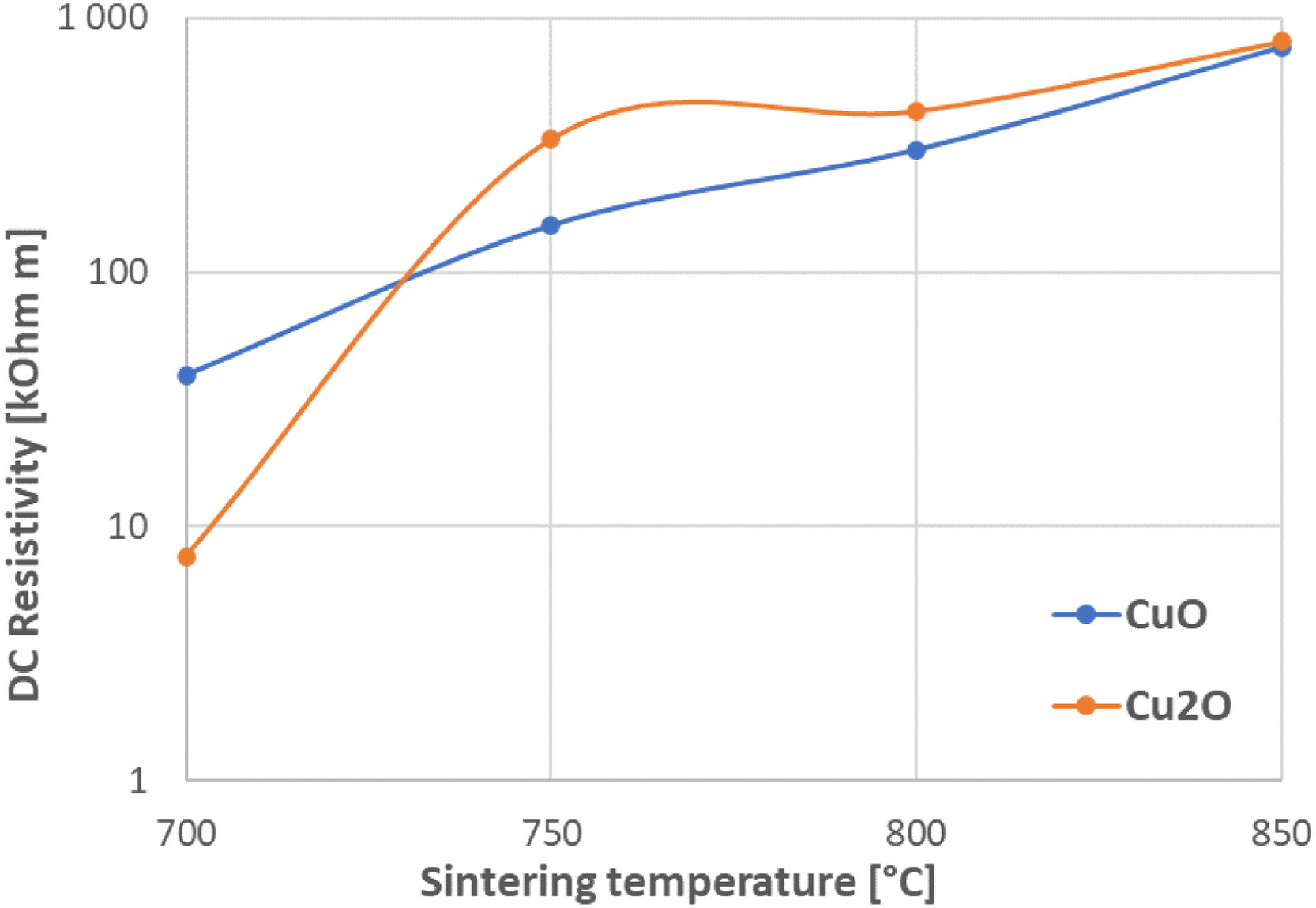
Electrical resistivityFig. 7 shows the DC resistivity for CuO and Cu2O samples sintered at different temperatures. For CuO the trend was straightforward and nearly linear – the higher the SPS temperature, the more resistive the sample was. The compaction process was probably slower for this material, and this could be considered as one important criterion (crystallite coarsening started after densification). Resistivity results for both oxides at 750°C and 800°C were very similar. The samples sintered at 850°C were again practically identical and a bit more resistive compared to lower temperatures. The published DC resistivity of CuO was in order of 2×10⁵Ωm [10]. Cu2O should theoretically be more conductive than CuO, but because of the coarse character of the Cu2O powder, its sintering optimum shifted to higher temperatures, and the resistivity of analogously sintered samples was similar for CuO and Cu2O.

If we consider the recording of air pressure in the SPS chamber, for the sample CuO-850, there was a higher difference between the “sintering dwell” conditions and the “experiment end” conditions. In the case of CuO-850, this difference was 162 arbitrary units whereas for Cu2O-850 it was only 96 arbitrary units. This speaks about the released gases, since the vacuum pumps worked continuously, and in the case of CuO, they had to suck-off more gas. Gas enclosed in pores in the case of CuO had higher volume, which was in consequence with the finer grains and limited compactness, c.f. Fig. 4.
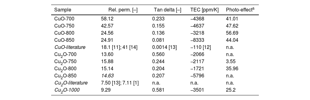
Permittivity and lossConcerning the relative permittivity at 1MHz and room temperature (the value can be found in literature), our CuO samples provided this trend: The highest is CuO-700 followed by CuO-750, whereas CuO-800 and CuO-850 had very similar and markedly lower values. The published value is in the case of CuO even lower, 18.1 [11]. The value of thermal coefficient of capacitance (TEC) is reported to be −110ppm/K for CuO [12]. Our CuO samples exhibited values between −3200 and −8300ppm/K. From both these standpoints, TEC and permittivity, the sample CuO-800 approached most closely the published values, however in the case of thermal coefficients, the actual SPS samples were substantially worse (i.e., a less thermally stable material).
A sample of Cu2O with roughly comparable microstructure was sintered in a furnace at 1000°C/4h dwell/air atmosphere. Its microstructure and detail dielectric study is not in focus of this article, but several values were added in Table 6 for comparison (label Cu2O-1000). Its permittivity was lover, losses higher, TEC value comparable and photo-conductance less pronounced compared to Cu2O-SPS. Let this be one indirect indicator that the processing window at SPS was approaching its optimal range.
Electrical properties at room temperature and frequency 1MHz.
| Sample | Rel. perm. [–] | Tan delta [–] | TEC [ppm/K] | Photo-effecta |
|---|---|---|---|---|
| CuO-700 | 58.12 | 0.233 | −4368 | 41.01 |
| CuO-750 | 42.57 | 0.155 | −4637 | 47.62 |
| CuO-800 | 24.56 | 0.136 | −3218 | 56.69 |
| CuO-850 | 24.91 | 0.081 | −8333 | 44.04 |
| CuO-literature | 18.1 [11]; 41 [14] | 0.0014 [13] | −110 [12] | n.a. |
| Cu2O-700 | 13.60 | 0.560 | −2066 | n.a. |
| Cu2O-750 | 15.88 | 0.244 | −2117 | 3.55 |
| Cu2O-800 | 15.14 | 0.204 | −1721 | 35.96 |
| Cu2O-850 | 14.63 | 0.207 | −5796 | n.a. |
| Cu2O-literature | 7.50 [13]; 7.11 [1] | n.a. | n.a. | n.a. |
| Cu2O-1000 | 9.29 | 0.581 | −3501 | 25.2 |
The reported bandgap of Cu2O was much higher than the value for CuO, 2.1eV and 1.1eV, respectively [13], which could also help with the answer why the photo-induced change of resistance of CuO was much higher in our study, see below.
Concerning Cu2O, these parameters are nearly absent in the literature, since this material is considered to be too much conductive. The only report is from the year 1973 [15], and gives permittivity of Cu2O as 7.50; another resource is an optical measurement of permittivity of a thin film [4], and it was 6.47. In our case, it was not exactly like this: Concerning the relative permittivity at 1MHz, our Cu2O samples were all between 13 and 16. Concerning the TEC parameter, calculated for our samples, Cu2O results were all around −2000ppm/K, with the exception of Cu2O-850, where the TEC value was nearly −6000ppm/K). Only the sample Cu2O-800 fitted the category of an X9R-capacitor concerning the temperature stability of permittivity (i.e. the difference between the permittivity value at room temperature and at 150°C, which must be lower than 15% of the maximum value [16,17]).
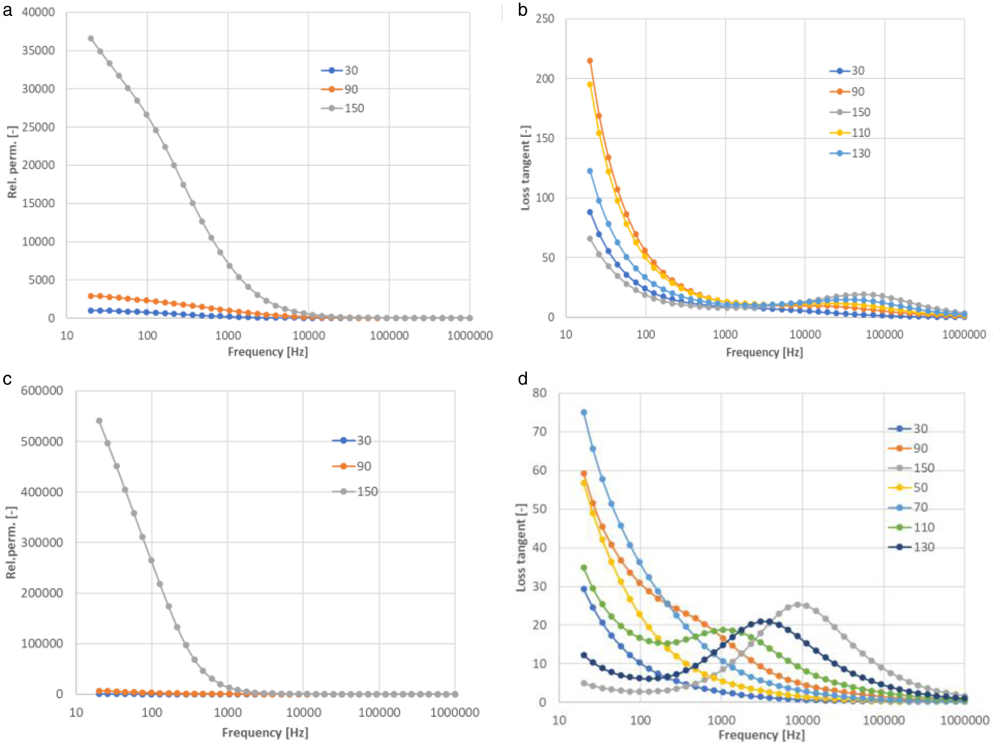
Existence of oxygen vacancies and grain boundaries as defects plays a key role in determining the dielectric behaviour of a material [8]. As the charge carriers reach the grain boundaries and accumulate at the interfaces, they result in net polarization. As the frequency of the applied field increases, the charge carriers begin to reverse the direction of their movement more often. Due to this fact the probability of electrons reaching the grain boundary decreases, which leads to a decrease in polarization. Therefore, ɛ′ decreased with increasing the frequency, where all the plots shown in Fig. 8 merge in the high frequency region irrespective of temperature.

Fig. 8 compares relative permittivity and loss tangent of CuO and Cu2O samples sintered at 750°C. At room temperature and also at 90°C, the relative permittivity looked very stable, whereas at 150°C it was strongly frequency-dependent. This holds for both CuO and Cu2O samples. Concerning the loss tangent, both materials were lossy at low frequencies. Both also exhibited a secondary peak, but for Cu2O, its characteristic frequency was higher, about 50kHz, compared to CuO, where it was between 1kHz and 10kHz.
From the data shown in Fig. 8, one can find that the dielectric response originated from a relaxation process and a low-frequency process. The former resulted in a giant value (∼105) of permittivity, Fig. 8a and c, in the low frequency range [18], and a high loss at certain frequencies (relaxation frequency, 20Hz to 1MHz in the temperature range studied). The relaxation frequency increased with the increasing temperature. The giant permittivity also increased with the increasing temperature. For example, the permittivity at 100Hz was about 300 at room temperature, and 5×10⁵ at 150°C. It can be noted in Fig. 8b and d that the loss tangent of CuO and Cu2O was high – above 25 at the relaxation peak – but only about 0.15 at its minimum, reached at the highest frequency of 1MHz.
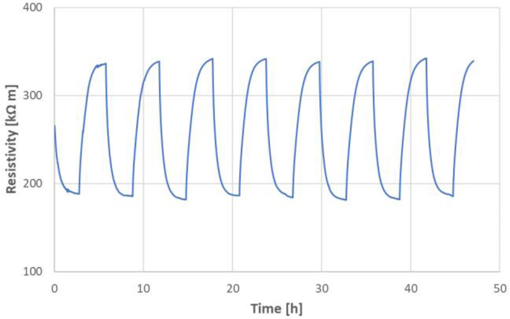
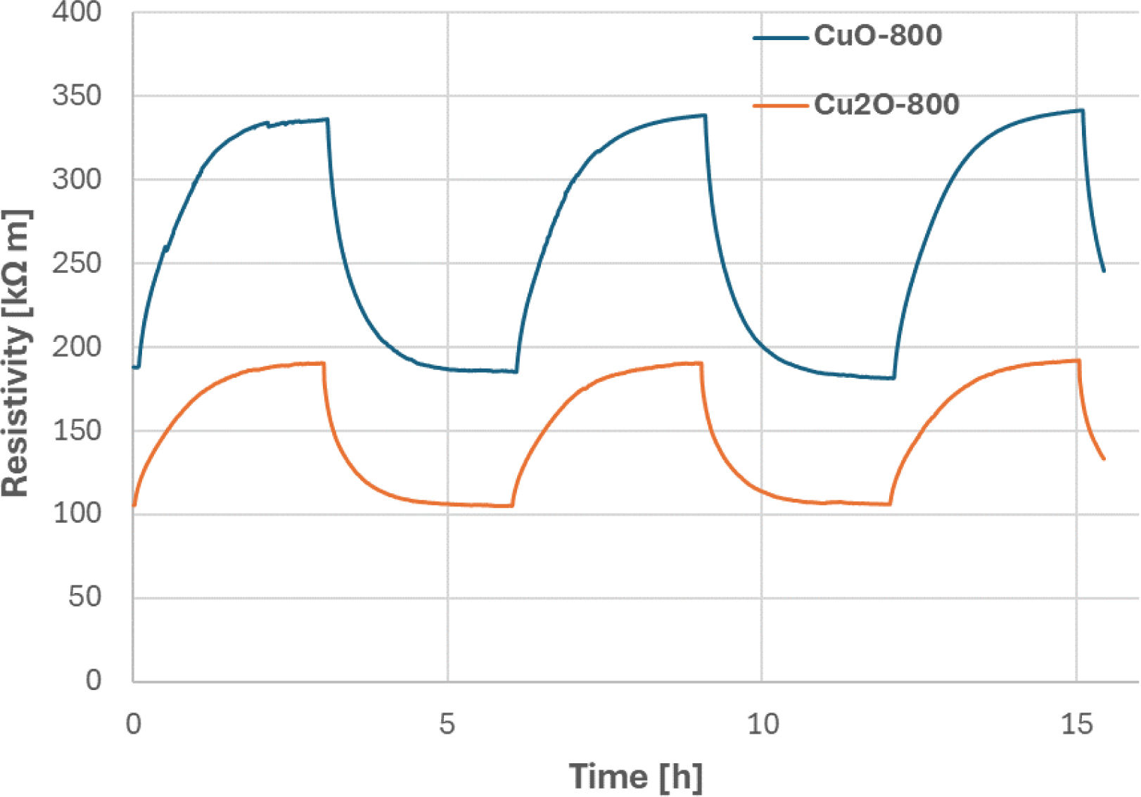
Photo-induced conductivityThe run of the DC resistivity was continuously monitored for 48h, Fig. 9. We saw a repeated rapid decrease of resistivity under illumination, which was always saturated after approximately 3h. This phenomenon corresponds to the activation of charge carriers and their subsequent depletion. Photoconductivity at room temperature could be mostly ascribed to the increment of carrier density under illumination. The new stable value of resistivity induced by light was at about 190kΩm, i.e., a decrease to about 44% of the initial value (i.e., a value just before enlightenment considered as 100%), c.f. also Table 6. After turning the light off, recovery started. This process was in our experiment similarly fast as the decay (approximately 3h). We can call this interval a persistent photoconductivity period. The initial “dark” value of 340kΩm was approached again. The experiment showed a rather large, but slow, fully recoverable photo-induced change of resistivity (or, inversely, conductivity). Similar transient photocurrent responses were detected at electrochemical measurements by other authors on a different ceramic material [19]. A high and persistent photoconductivity at an oxide-based heterostructure was also described [20]. The reproducibility of the photoconduction phenomenon was monitored for 48h of the total duration. The light-on periods were characterized by the resistivity value between 188kΩm and 192kΩm, whereas the light-off periods exhibited the resistivity value between 338kΩm and 342kΩm.

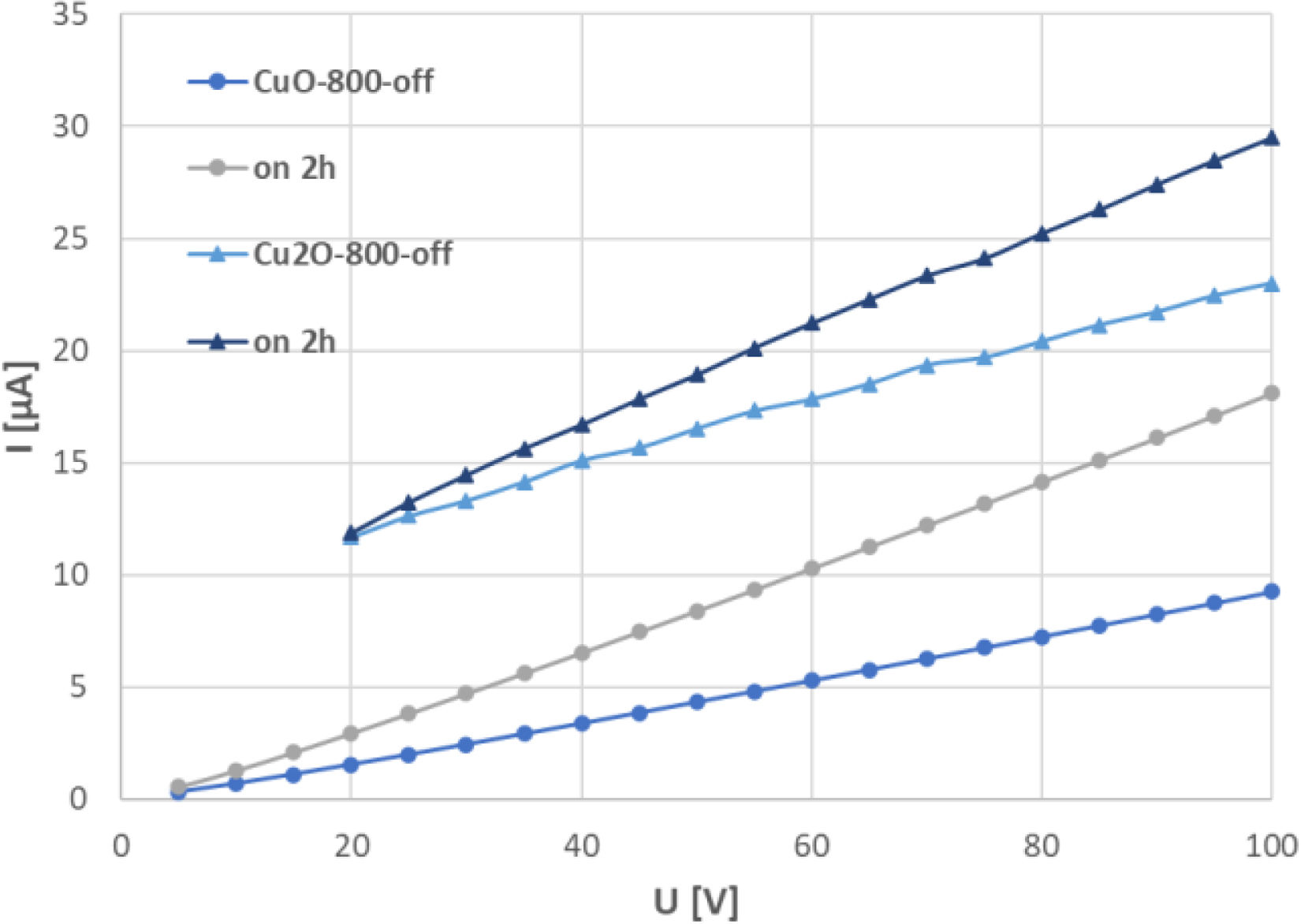
A graph showing the volt-ampere characteristics (VAC), Fig. 10, presents the current in microamperes when the voltage was swept from 0 to 100V DC with a step of 5V and a time step of 10s. Two samples are shown, CuO-800 and Cu2O-800. The VAC for the dark conditions is labelled “off” and the VAC recorded with a sample conditioned under the light for 2h is labelled “on 2h”. The graph shows that the stronger the voltage, the more pronounced the light-induced photo-conductance, and the phenomenon was strictly linear. This linearity would be perfect for a sensor function of the material. A comparison of the samples CuO-800 and Cu2O-800 showed that for the CuO sample, this linearity was maintained for the whole observed range, whereas for the Cu2O sample the trend was linear followed only over 20V. Under 20V the response was rather logarithmic (not shown). An intrinsic electrostatic barrier at the grain boundaries is attributed to be responsible for the nonlinear VAC behaviour [21]. In our case, this was the behaviour of Cu2O between 5V and 20V.

To compare behaviour of CuO-800 with Cu2O-800, measurements of the photoconductivity were performed for a 16-h duration, Fig. 11. The intervals of dark and light periods were identical. Concerning the comparison between CuO and Cu2O, the “dark” resistivity value was different, 340kΩm for CuO-800 and 190kΩm for Cu2O. The difference between maximum and (light-induced) minimum was 44% for both CuO and Cu2O. We can conclude that both materials have the same intensity of response to the enlightenment, the same decay duration and also the same recovery duration.
Discussion
Dielectric loss is the energy loss in the form of heat in the dielectric material at varying applied AC field. Relaxation polarization loss and conduction loss are the two main mechanisms that may dissipate energy within a dielectric material.
The real part of the relative permittivity exhibited a strong decrease at frequencies in the range from 50Hz to 1000Hz, with a loss peak accompanying them. The loss peak showed a continuous trend of shifting towards high frequencies at high temperatures. The peak was preceded by an initial decrease of the loss tangent, which was proportional to the frequency. This decrease of the loss tangent was observed only in the low frequency range from 20Hz to 1000Hz, and this range was extended with the temperature. No significant change was detected in the width of the peak with the temperature. The negative slope of the low frequency dispersion curve suggested a conduction-dominated loss at a low frequency.
The enormously high value of ɛ′ at very low frequencies is attributed to the build-ups of charge carriers at the Cu2O [22] grain boundaries. This phenomenon is known as the Maxwell–Wagner effect. At higher frequencies, ɛ′ approaches a constant value, because dipoles cannot follow the rapid variation of the AC electric filed. This phenomenon was seen in both our samples Cu2O and CuO.
The dielectric dispersion was not explainable by assuming the homogeneous system, and instead, there might have been various components, which contributed individually to the dielectric response. One possible combination could be the usual grain and grain boundary (series) combination, each component being a parallel combination of capacitance and resistance. This is the equivalent to Maxwell–Wagner (M–W) type relaxation, where additional capacitance comes from extrinsic sources such as grain/grain-boundary charge accumulation. The high permittivity of CuO ceramics is attributed to the reduction in resistance due to Cu/O defects in the grain by the (M–W) mechanism [23].
The loss tangent peak corresponds approximately to the situation where the grains contribute mainly to the resistance, and the grain boundaries contribute only to the capacitance. This becomes a series resistance–capacitance (RC) circuit at that frequency range when the grain boundary capacitance dominates the impedance of the grain boundary, but the grain impedance is still governed by the resistance of the grains.
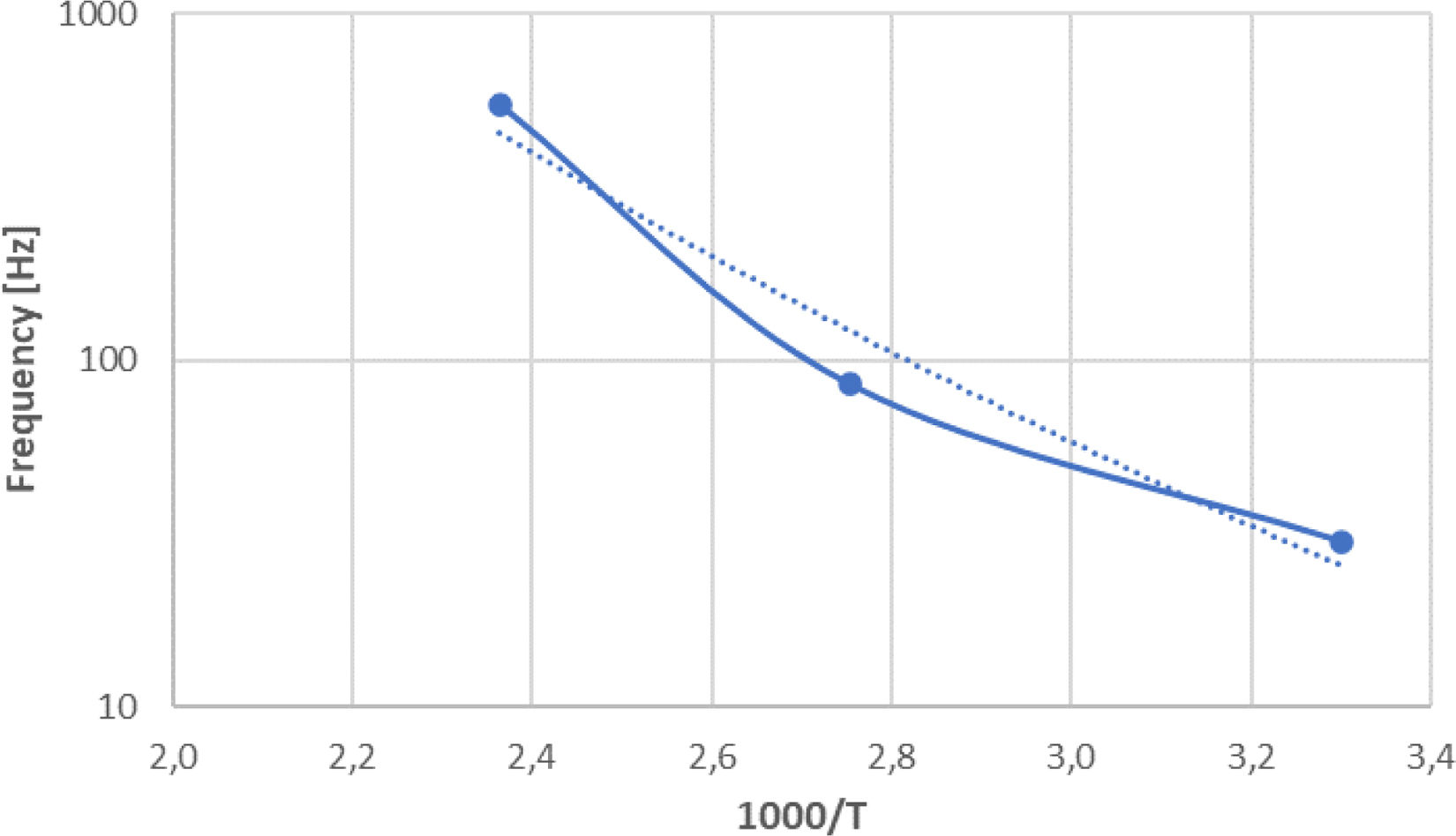
As temperature decreased, permittivity dropped also at low frequencies, and corresponding dielectric loss peaks were observed at the same frequencies, which can be explained by the Debye relaxation theory [24]. Fig. 12 displays the Arrhenius plot (sample Cu2O-750) of the peak frequency in the impedance, which was approximately linear at a high temperature. The corresponding activation energy was 0.90eV. The width of the peak was 1.73 decade, confirming the non-Debye type relaxation at high frequencies, where the peak width should be 1.14 decade [25].

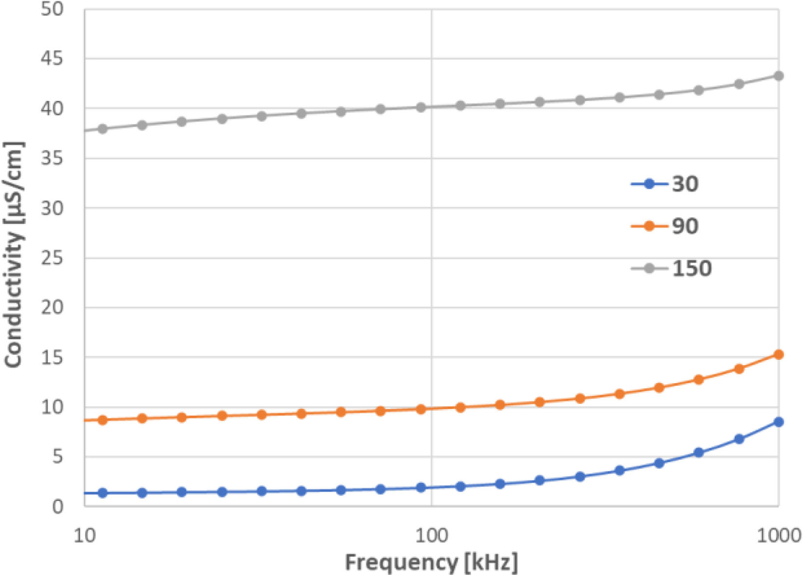
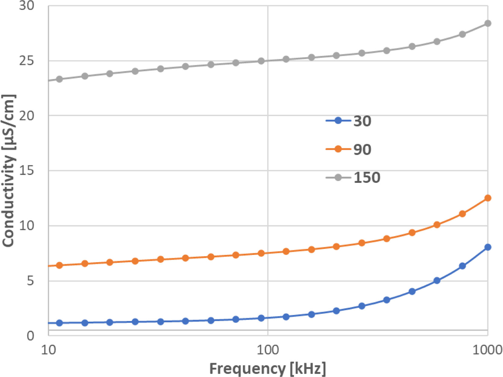
A closer investigation of the AC conductivity (σac) versus (f) curves, Figs. 13 and 14, showed that it can be characterized by three frequency regions with different slopes; (s1) under 50kHz; (s2) 50–500kHz; (s3) 500kHz–1MHz. This sort of behaviour was mainly pronounced at 30°C.


From the R.T. curves it is evident that, at low frequencies, the AC conductivity was almost frequency independent, which was a consequence of a DC leakage current throughout the sample and was only dependent on the voltage applied. At higher frequencies, the AC conductivity increased.
A reasonable agreement between the conductivity calculated based on DC resistance measurement and between that based on impedance analysis existed. For example, the sample CuO-800 had, at room temperature and 20Hz, the AC conductivity equal to 6.85×10⁻⁸S/cm, whereas DC conductivity 1.30×10⁻⁸S/cm. This is also in concordance with the general trend of increasing conductivity with an increasing frequency. For the other samples, the differences were similar. The total conductivity (σ) increased with temperature due to the increase in the number of the charge carriers and thermal agitation. Transition from the low to the high frequency regions occurs at a critical frequency called the hopping frequency [22], that shifts to lower frequencies with increasing temperature. The change in behaviour of the hopping frequency from flat to rapidly rising may be related to a change in the hopping behaviour of charge carriers from a short range (s3) to a long range (s2).
Our conclusion is that inside the grains, both electrons and oxygen vacancies dominated the conduction, and electronic conduction was the major contributor in the grain boundary regions – for both CuO, similarly to [26], and also Cu2O materials. At low temperatures near the room temperature, the electric dipoles cannot orient themselves along the direction of the externally applied field, and, therefore, their contribution to the polarization and the dielectric permittivity was weak. When the temperature increased, the bound charge carriers received enough thermal energy to be able to follow the change in the field orientation more easily. This, in turn, enhanced their contribution to the polarization leading to an increase in permittivity. The increasing peak position and the increase in its maximum value indicated thermally generated contribution [27] to the losses.
Concerning the microstructure aspects, Cu2O with its markedly coarser grains had the loss tangent peaks at higher frequencies. This, however, could be associated with lower open porosity of this material when sintering is done at a high temperature. Large dipoles of water molecules or other hydrated components, present possibly in certain fraction of pores, could shift the loss peak to a lower frequency in the case of CuO samples.
ConclusionsTenorite CuO and cuprite Cu2O commercial powders were consolidated to form a ceramic bulk via spark plasma sintering (SPS). The resulting samples’ microstructure was isotropic and rather homogenous, however, with certain porosity. The phase purity was better preserved in the case of CuO. No grain coarsening was detected in the studied processing temperature window 700–850°C.
All sintered compacts were dielectrics with higher relative permittivity and higher loss tangent than typical available literature values of the copper oxides. On the other hand, they had a purely resistive character. Sintered samples exhibited a two-slope course in permittivity and, correspondingly, two-fold maxima on loss curves versus frequency – the first one at very low frequencies, and the second one at about tens of kilohertz. These phenomena were pronounced with the increasing measurement temperature. Up to 100°C both studied oxides represented rather adequate dielectric behaviour (relative permittivity 20, loss tangent 0.1, thermal coefficient of capacitance −3000ppm/K). Above this temperature, they became giant-polarization materials. The difference between CuO and Cu2O from the electrical standpoint was finally not so dramatic as the stoichiometry indicated.
Both types of oxides exhibited light-induced photo-conductance with a persistent character. The photo-current flow was always stronger under the influence of the visible light irradiation, and samples had, at the same time, a linear response to voltage in the range from 20V to 100V DC. Such behaviour seems useful in sensor application.
The work at The Czech Academy of Sciences, Institute of Plasma Physics was supported by the project 101120555—CLiCAM—HORIZON-WIDERA-2022-TALENTS-03.