Ferroelectric materials have attracted significant attention in recent decades because they can be used in various electronic devices. BiFeO3 (BFO) has a perovskite-type ABO3 structure with antiferromagnetic and ferroelectric properties and a band gap within the visible light range, making it a promising candidate for use in sensors and solar cells. In this study, BiFeO3 thin films were grown by radio frequency (RF) sputtering using a homemade target and sintered at different times to evaluate the influence of sintering time on their physical properties. Its physical properties were evaluated using X-ray diffraction (XRD), scanning electron microscopy (SEM), and Raman spectroscopy. These results revealed that all films maintained a perovskite-like structure with rhombohedral and bismuth-rich secondary phases (Bi2O2.33). Atomic force microscopy (AFM) and piezoresponse force micrography (PFM) images depicted the impact of sintering time on surface roughness and ferroelectric domain reorientation. The optical properties, such as n, k, and the band gap of all samples, were obtained using reflection-transmission spectroscopy. The photoresponse under dark, visible and UV illumination were evaluated on BFO films grown over glass-FTO substrate.
Los materiales ferroeléctricos han atraído gran atención en las últimas décadas porque pueden utilizarse en diversos dispositivos electrónicos. El BiFeO3 (BFO) tiene una estructura ABO3 de tipo perovskita con propiedades antiferromagnéticas y ferroeléctricas y una banda prohibida dentro del rango de luz visible, lo que lo convierte en un candidato prometedor para su uso en sensores y celdas solares. En este estudio, películas delgadas de BiFeO3 crecieron mediante erosión catódica por radiofrecuencia utilizando un blanco casero y se sinterizaron durante diferentes tiempos para evaluar la influencia del tiempo de sinterización en sus propiedades físicas. Sus propiedades físicas se evaluaron mediante difracción de rayos X (XRD), microscopia electrónica de barrido (SEM) y espectroscopia Raman. Estos resultados revelaron que todas las películas mantenían una estructura del tipo perovskita ABO3 con fase romboédrica y una fase secundaria rica en bismuto (Bi2O2.33). Las imágenes de microscopia de fuerza atómica (AFM) y microscopia de fuerza de respuesta piezoeléctrica (PFM) mostraron el impacto del tiempo de sinterización en la rugosidad de la superficie y reorientación de dominios ferroeléctricos. Las propiedades ópticas, como n, k y la banda prohibida de todas las muestras, se obtuvieron mediante espectroscopia de reflexión-transmisión. La fotorrespuesta bajo iluminación visible, UV y sin iluminación (oscura) se evaluó en películas de BFO depositadas sobre sustrato de vidrio-FTO.
Bismuth ferrite (BiFeO3 or BFO) is a ferroelectric material with an ABO3 perovskite-type structure that has attracted much attention in recent decades due to its high phase transition temperatures (Neel and Curie temperatures), which make it a very promising material due its antiferromagnetic and ferroelectric properties at room temperature, a high dielectric constant, and its band gap is within the visible light range [1]. However, there are some major drawbacks in the synthesis of this material: The difficulty of obtaining it free of secondary phases, the presence of a spin cycloid that blocks the magnetic response and the high leakage current, which makes it very difficult to fully exploit its hypothetical ferroelectric behavior at room temperature [2,3]. Even more, there are some contributions in which the ferroelectric response has only been observed in doped BFO thin films at liquid nitrogen temperature [4]. The crystalline structure of this material is strongly related to its piezoelectric, pyroelectric, and ferroelectric properties. Additionally, BFO is environmentally friendly because it does not contain lead (Pb). Therefore, it is a potential candidate for replacing lead-based materials in electronic devices, such as sensors, actuators, photodetectors, and photovoltaic devices. The properties of these materials depend on the synthesis parameters [5]. The effect of heat treatment on the physical properties of ferroelectric materials has been analyzed for different systems [3–6]. Ayala et al. reported a change in the band gap of BFO powders at different sintering times and temperatures (2.36eV without heat treatment, 2.11eV, and 2.19eV at 500°C for 8h 50min, and 600°C for 10h 30min, respectively) [6]. The heat treatment effect on the stability and formation of secondary phases of BFO powders obtained by sol–gel at different temperatures has been studied, and it was observed that the sample treated at 450°C showed more significant suppression of secondary phases than the rest of the samples [7]. BFO thin films via sol–gel were deposited and thermally treated at 450, 500, and 550°C for 2h. Structural parameters such as crystal size (15.2–41.2nm), roughness (1.847–5.239nm), and band gap (2.83–2.65eV) were affected as the sintering temperature increased [8]. In sol–gel thin films, samples sintered at 300°C were mostly composed of secondary phases, however, when treated at 600°C the BiFeO3 phase was observed along with the secondary phases [9]. The effect of sintering temperature on thin films deposited by RF sputtering has been studied [10–12]. BFO thin films deposited by RF sputtering and sintered at 500–700°C showed that the BFO is mostly observed at 600°C, with secondary phases such as Bi2SiO5 and Bi2Fe4O9 present in all samples [10]. However, the influence of sintering time on the physical properties, such as structural, ferroelectric, and optical in BFO thin films deposited by RF sputtering has not been widely studied. In this study, BFO thin films were deposited on glass and FTO substrates by RF sputtering from a ceramic target synthetized in our laboratory, free of secondary phases. Subsequently, they were sintered ex situ in atmospheric conditions at 550°C for 30, 45, and 60min. The effect of sintering time at constant temperature on its structural, ferroelectric, optical, and photoresponse properties were studied.
Material and methodsBiFeO3 thin films were deposited via RF cathodic erosion using a homemade ceramic target of 2 in diameter fabricated with a modified solid-state reaction route. To manufacture the target, high-purity oxide powders (Bi2O3, Sigma–Aldrich 99.9% and Fe2O3, Sigma–Aldrich 99%) were used in stoichiometric proportions with a 5% excess of Bi to mitigate its volatilization. These were ground using a SPEX/mixer mill 8000 for 1 hour and subsequently uniaxial pressed using a hydraulic press under a pressure of 93MPa. The pressed powders were subjected to a thermal treatment consisting of calcination at 820°C for 90min and then sintered at 850°C for 90min at air atmosphere without a second grinding process.
The growth of the BFO films consists of 3 layers on commercial Corning glass and FTO substrates. This process is done to prevent the formation of superficial cracks in the films during sintering, improve the nucleation surface and achieve a thickness close to 200nm [13]. The deposition time for the first layer was 10min, the second layer was deposited for 30min, and the third layer for 50min, all layers were deposited at 2.47W/cm2 of power at room temperature. During the synthesis of films each layer was subjected to ex situ sintering in atmospheric conditions at 550°C at a heating rate of 10°C/min using different times of heat treatment.
The sintering times were 30, 45, and 60min, labeled as BFO30, BFO45, and BFO60, respectively. Finally, graphite contacts of 700μm of diameter using graphite paint were deposited on all films to study electrical properties. A Lindberg ISB furnace was used for sintering. The crystalline structure was determined by X-ray diffraction using a RIGAKU Dmax 2100 diffractometer with a CuKα source (λ=1.5406Å). The measurement range was carried out at 20–80° in 2θ with a step of 0.02° and 0.4 s per step. Crystalline phase concentrations, lattice parameters, and crystallite size were determined by Rietveld refinements using MAUD software. The surface morphology of thin films was obtained via SEM using a Philips XL30 ESEM scanning electron microscope. Raman spectra were obtained using a Horiba Jobin Yvon, DilorII Microraman spectrometer with He–Ne laser excitation line with a wavelength of 632.8nm. Atomic force microscopy was conducted using a Bruker Nanoscope IV Dimension 3100 atomic force microscope to assess roughness, and a conductive tip was used to obtain Piezoresponse Force Microscopy (PFM) images. The reflection and transmission spectra for the analysis of optical properties were obtained on a Film Tek 3000 UV-Vis spectrometer in a range of 300–850nm. An Agilent 4255C semiconductor parameter analyzer was used to measure current vs voltage (I–V) curves in dark and illumination conditions, with UV lamp (365nm) and visible illumination LED lamp (420–700nm).
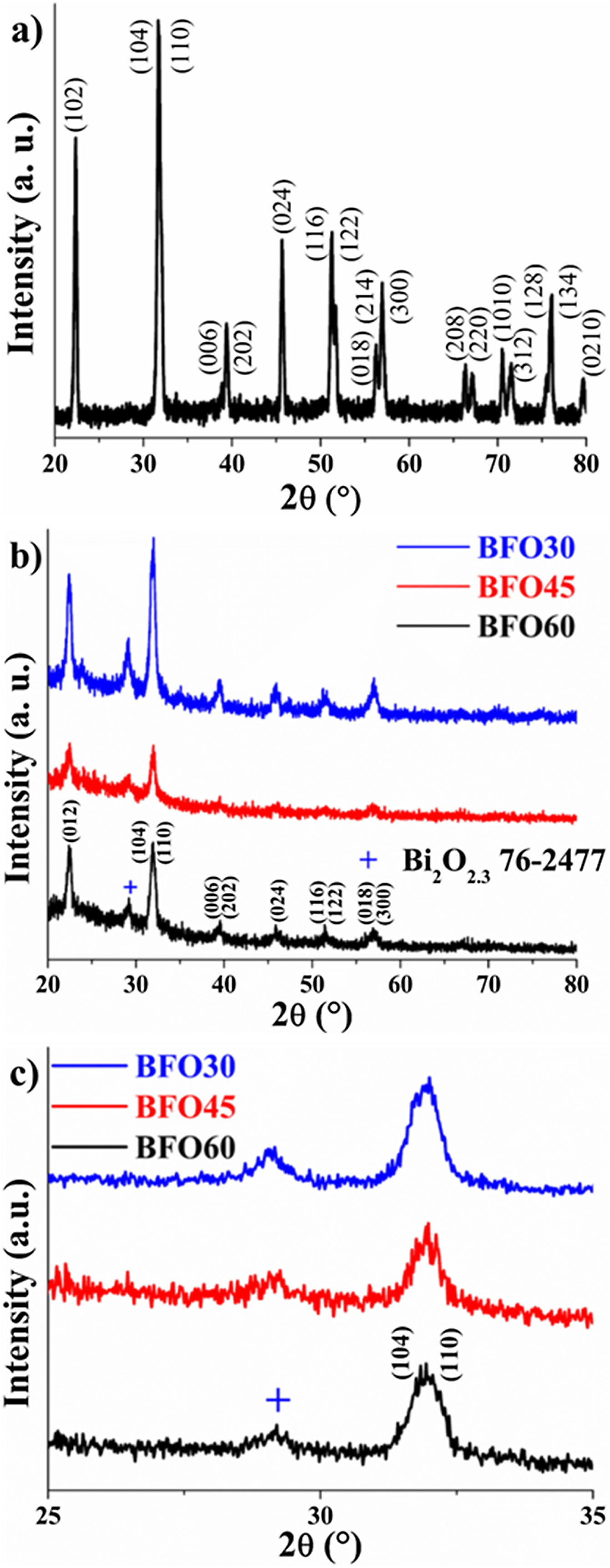
Results and discussionX-ray analysisFig. 1a shows the X-ray diffraction pattern of the sintered ceramic target in the range of 20–80° in 2θ. All peaks matched the crystallographic PDF #71-2494, corresponding to BiFeO3 with a perovskite-type rhombohedral R3c (161) structure without secondary phases. The absence of secondary phases in the target is attributed to the addition of 5% excess Bi in the synthesis stage. This element volatilizes easily at temperatures above 800°C and BiFeO3 is very susceptible to forming secondary phases due to excess or deficiencies of Bi [14]. Therefore, the modified solid-state reaction route of the ceramic target to obtain a single perovskite phase without secondary phases was successful. Fig. 1b shows the diffraction patterns of BiFeO3 thin films treated at different sintering times (BFO30, BFO45, and BFO60) on glass substrates in a range of 20–80° in 2θ. The diffraction peaks of all the samples matched with the PDF-86-1518 corresponding to BiFeO3 with a perovskite-type structure with a rhombohedral phase. All films contain the secondary phase of Bi2O2.33 (“+” in the figure) around 29° in 2θ. The precipitation of Bi is attributed to the pressure and temperature conditions used during deposition [15]. In Fig. 1c, an enlargement of the normalized principal peak between 25° and 35° in 2θ is shown, where it is evident that the position and shape of the peak remain unchanged. The above indicates that all samples possess the same rhombohedral R3c phase.
The lattice parameters were determined by Rietveld refinement using MAUD software (Table 1), revealing a subtle change in the “a” and “c” lattice parameters, increasing from 5.5855Å to 5.6102Å in “a” and decreasing from 13.8510Å to 13.7382Å in “c” as sintering time increased in the thin films. The crystal size decreased as the sintering time increased, from 14.74nm to 12.52nm. The percentage of the Bi2O2.33 secondary phase was quantified. These results indicate that samples sintered for 30 and 60min have the lowest amount of this phase (23.2% in each sample). The BFO30 and BFO60 films exhibit higher intensity diffraction peaks than the BFO45 sample, this is due the high concentration of the secondary phase causes greater intensity in the peaks corresponding to this phase, which mitigates the intensity of the peaks corresponding to BiFeO3. These non-sequential changes without clear trend are consistent with the thermal instability characteristic of BiFeO3-based materials, where the structural, electrical, ferroelectric, and optical properties are influenced by heat treatments [10–13].
Refined structural parameters of BFO target and thin films using MAUD.
| Samples | BFO target | BFO30 | BFO45 | BFO60 |
|---|---|---|---|---|
| R3c (%) | 100.0 | 76.8 | 50.4 | 76.8 |
| a (Å) | 5.5825 | 5.5855 | 5.5972 | 5.6102 |
| c (Å) | 13.8711 | 13.8510 | 13.7558 | 13.7382 |
| CZ (nm) | 20.64 | 14.74 | 14.10 | 12.52 |
| Bi2O2.33 (%) | – | 23.2 | 49.6 | 23.2 |
| a (Å) | – | 3.8436 | 3.8577 | 3.8301 |
| c (Å) | – | 35.8184 | 36.5993 | 35.8702 |
| CZ (nm) | – | 12.43 | 12.46 | 10.18 |
| Σ | 2.02 | 1.69 | 1.72 | 1.66 |
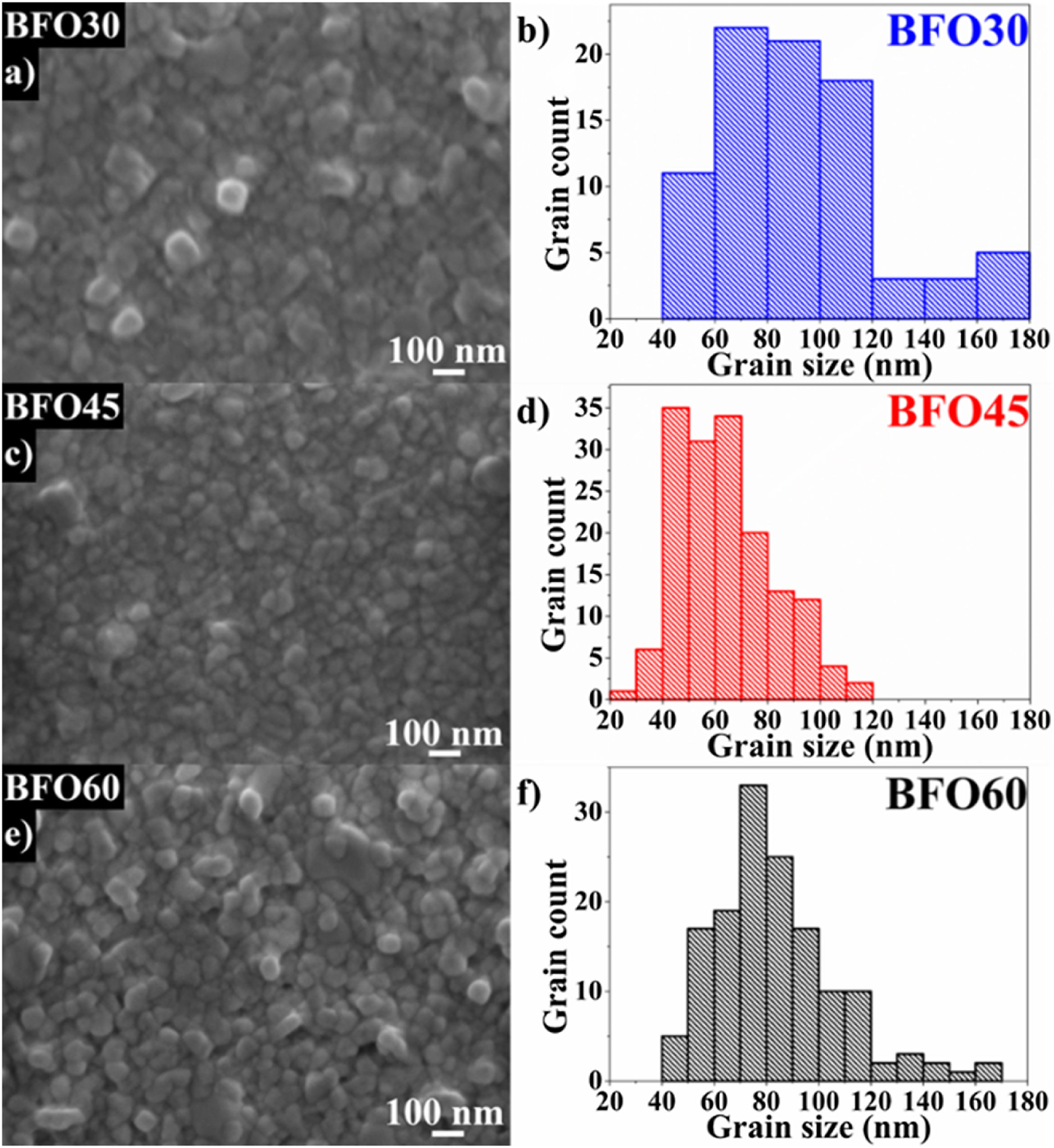
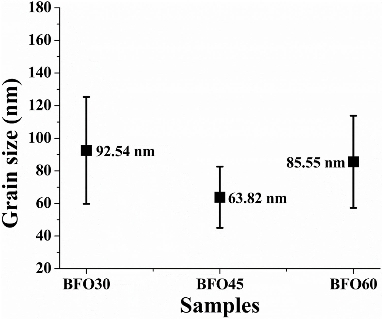
The surface micrographs (75,000×) of thin films of BFO at different sintering times (Fig. 2a, c, and e) show the granular morphology in each sample. Dense thin films are observed, with well-defined grains and no surface cracks. The morphology changes with the sintering time for each sample. The matrix average grain size (Fig. 3b, d, and f) is 92.54nm, 63.82nm, and 85.55nm, and the standard deviation is 32.78nm, 18.77nm, and 28.28nm for BFO30, BFO45, and BFO60, respectively. A trend of grain size reduction was observed for all the films, with a notable drop in BFO45. Furthermore, larger grains with a brighter tone in all films correspond to agglomerations of bismuth oxide (Bi2O2.33), confirming the results obtained from X-ray patterns and the Rietveld analysis. The presence of secondary phases can influence the suppression of grain growth in ferroelectric materials [14,15]. In our case, the presence of a bismuth-rich phase (Bi2O2.33) leads to a reduction in grain size. The sample with the highest concentration of the secondary phase exhibits the smallest grain size (BFO45) [16,17].
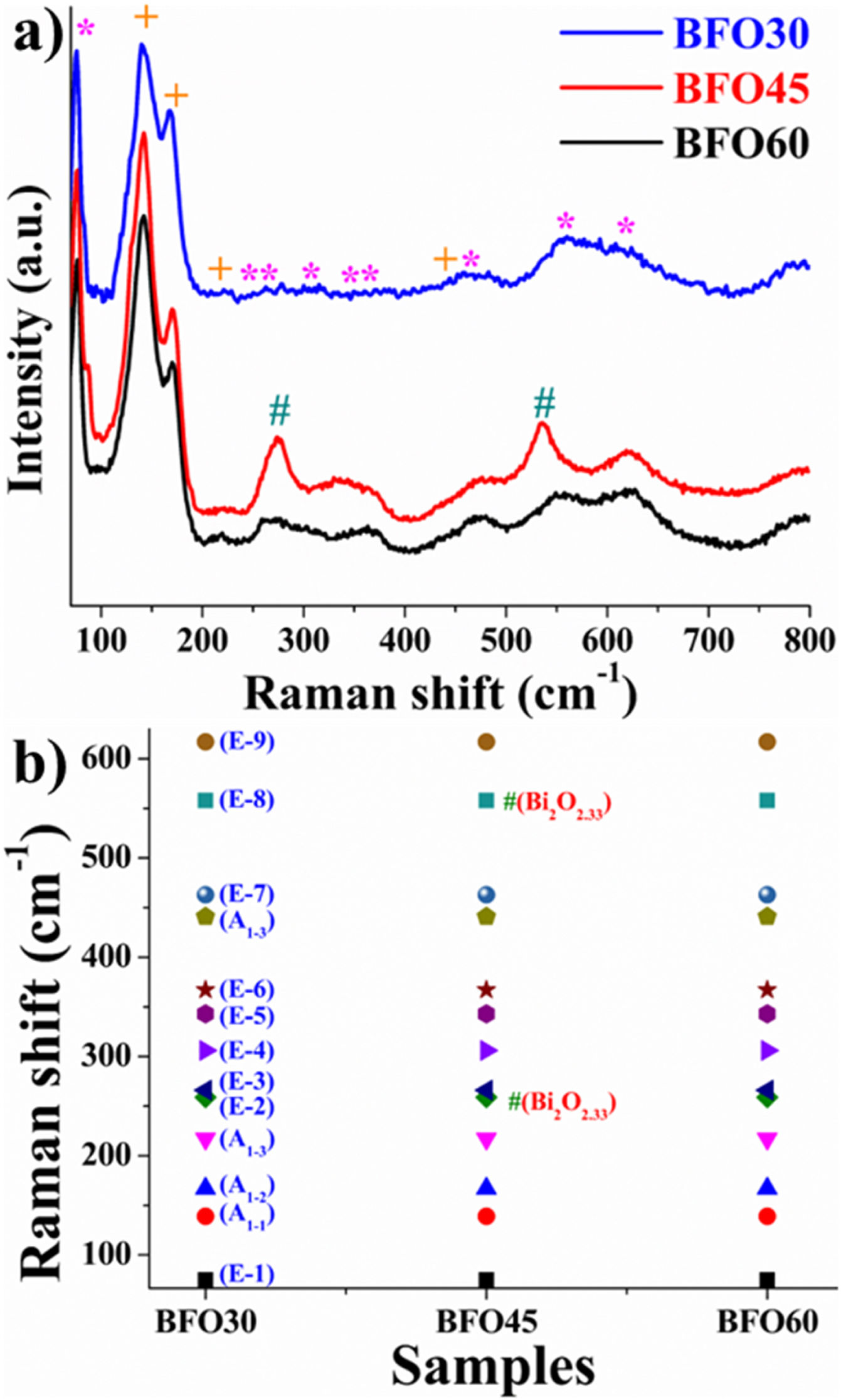
Fig. 4a shows the room temperature Raman spectra of BiFeO3 thin films sintered at different times. Group theory predicts 13 active Raman modes for rhombohedral distorted BFO in the R3c symmetry, Γ=4A1+9E [18]. 13 Raman modes for the sintered BiFeO3 thin films at different times (BFO30, BFO45, and BFO60) were distinguished. In general, the A1-1, A1-2, A1-3, and A1-4 modes (+) are distinguished at approximately 139cm−1, 167cm−1, 217cm−1, and 441cm−1 respectively, along with 9 E modes (*) at around 75cm−1, 259cm−1, 266cm−1, 306cm−1, 343cm−1, 367cm−1, 463cm−1, 558cm−1, and 617cm−1 (Fig. 4b). These modes were fitted according to studies of Kothari et al. of rhombohedral BiFeO3 in the R3c symmetry [19]. It has been reported that the low-frequency modes are associated with the vibration of BiO bonds [20], and the high-frequency modes are attributed to FeO bonds. As the sintering time increases, the modes observed in the range from 217cm−1 to 441cm−1 increase in intensity and definition. This is clearly observed when comparing BFO30 with BFO45 and BFO60, where the modes A1-3, E-2, E-3, E-4, E-5, E-6, and A1-4. All of the above indicates structural distortions as time increases [21]. The Bi2O2.33 phase (#) appears as expected according to the results obtained through X-ray diffraction (DRX) and Rietveld analysis. In BFO45, two prominent peaks around 272cm−1 and 534cm−1 are observed, which corresponds to Bi2O2.33 and is not present in the other samples [21,22].
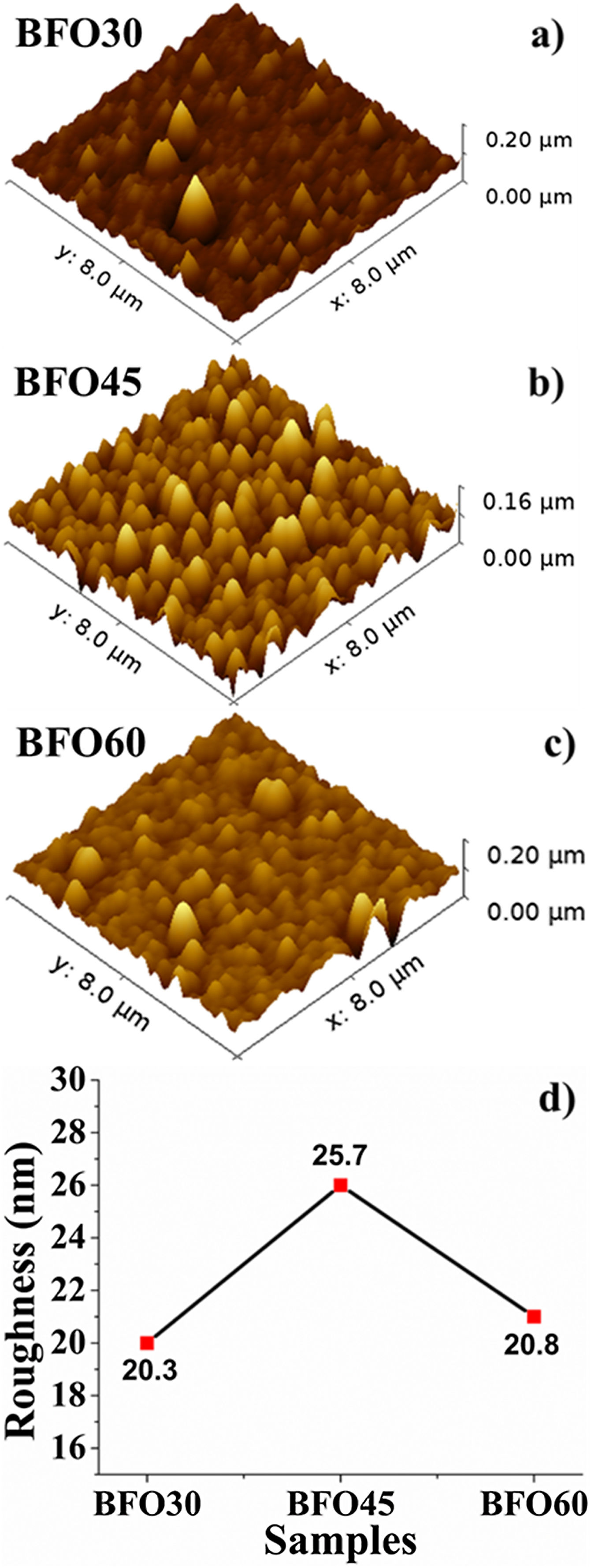
AFMThe atomic force microscopy images of BFO thin films at different sintering times show the topography of each sample (Fig. 5a–c). The roughness changes with sintering time: 20.3±0.095nm, 25.7±0.080nm, and 20.8±0.072nm for BFO30, BFO45, and BFO60, respectively. Some columnar-like growth is observed in all films; this is common in thin films of BiFeO3 grown by RF sputtering [18–21,23], significantly impacting the roughness of thin films deposited by this technique. It has been reported that the deposition of bismuth oxide (Bi2O3) by RF sputtering can acquire the texture of nanotubes, so the high concentration of this secondary phase can promote columnar growth [24], which causes a difference in roughness due to the presence of different phases as seen in all samples. These results explain the observed roughness behavior (Fig. 5d), as the film with a higher concentration of bismuth oxide phase (BFO45) has a higher concentration of columns per unit area than those with a lower concentration of this phase (BFO30 and BFO60).
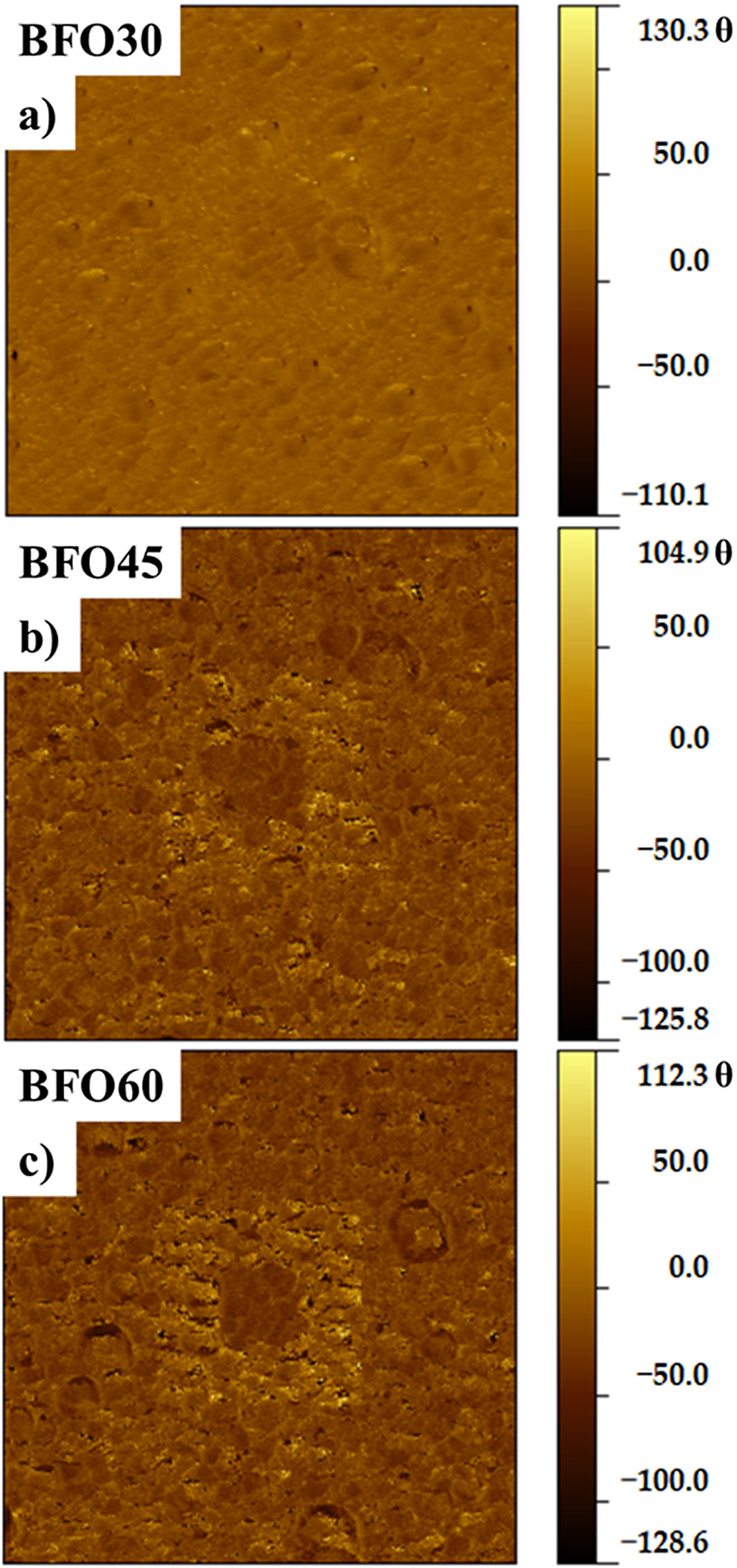
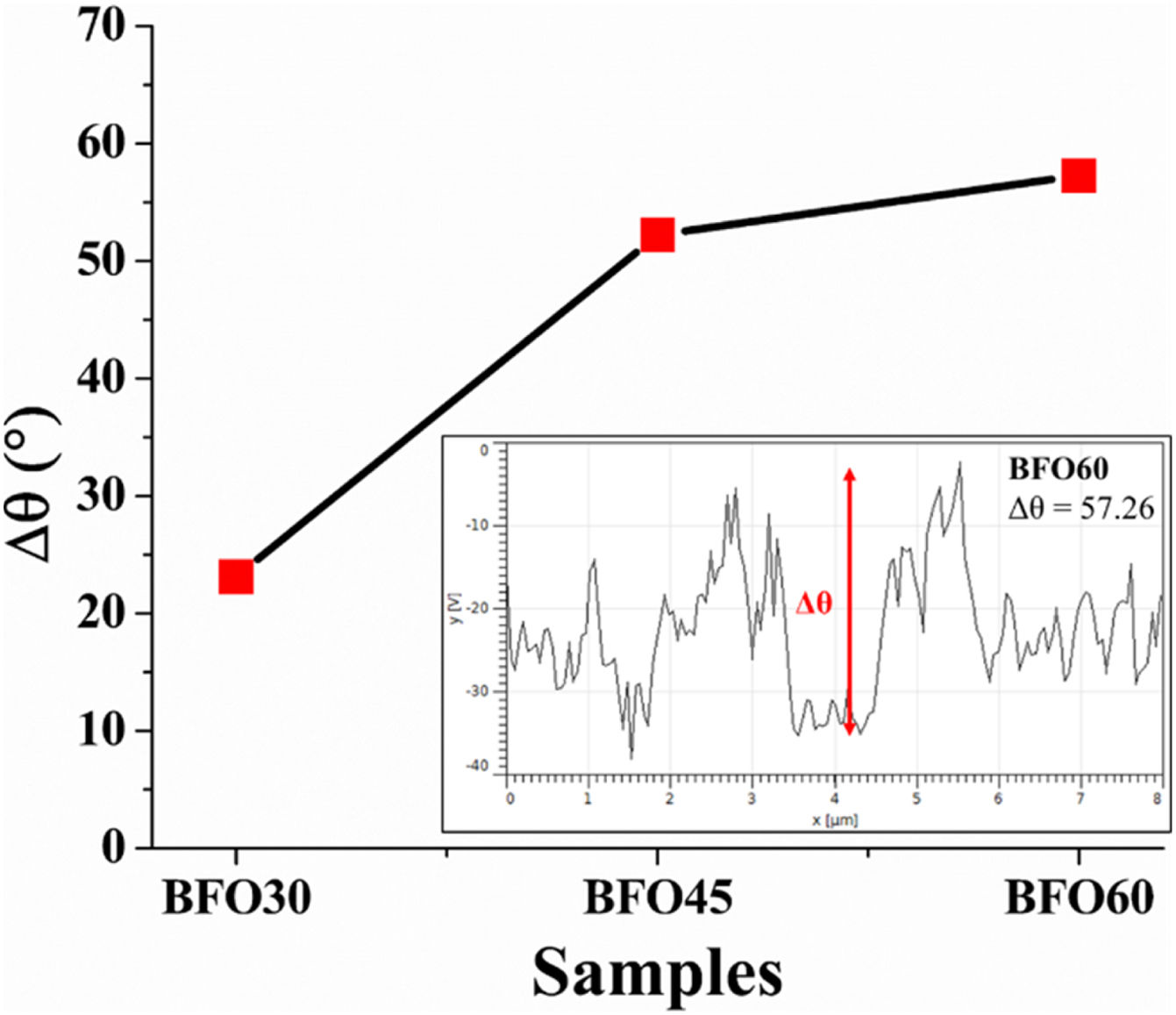
PFMThe structure of ferroelectric domains was studied by piezoresponse force microscopy (PFM), where out-of-plane phase micrographs were obtained (Fig. 6a–c). The tone contrast is due to the difference in direction of the polarization vector, indicating a random polarization of ferroelectric domains despite the current leakage common in this material. This is unequivocal evidence of the presence of ferroelectric domains in all samples. The reorientation of ferroelectric domains in all samples of the BiFeO3 system treated at different sintering times was achieved, as observed in the contrast difference due to changes in the direction of the polarization vector [25–27]. The ferroelectric domain polarization reversal was achieved by applying a voltage of ±9V to areas of 3μm×3μm and 1μm×1μm. The domain reorientation increased as the sintering time increased from 30min to 60min (Fig. 7). The above was determined based on the Δθ (Fig. 7 inset, Gwyddion V. 2.36 program) between the regions polarized at +9V and −9V [28]. All samples exhibit the ferroelectric characteristic of domain reorientation, where Δθ is strongly influenced by the sintering time.
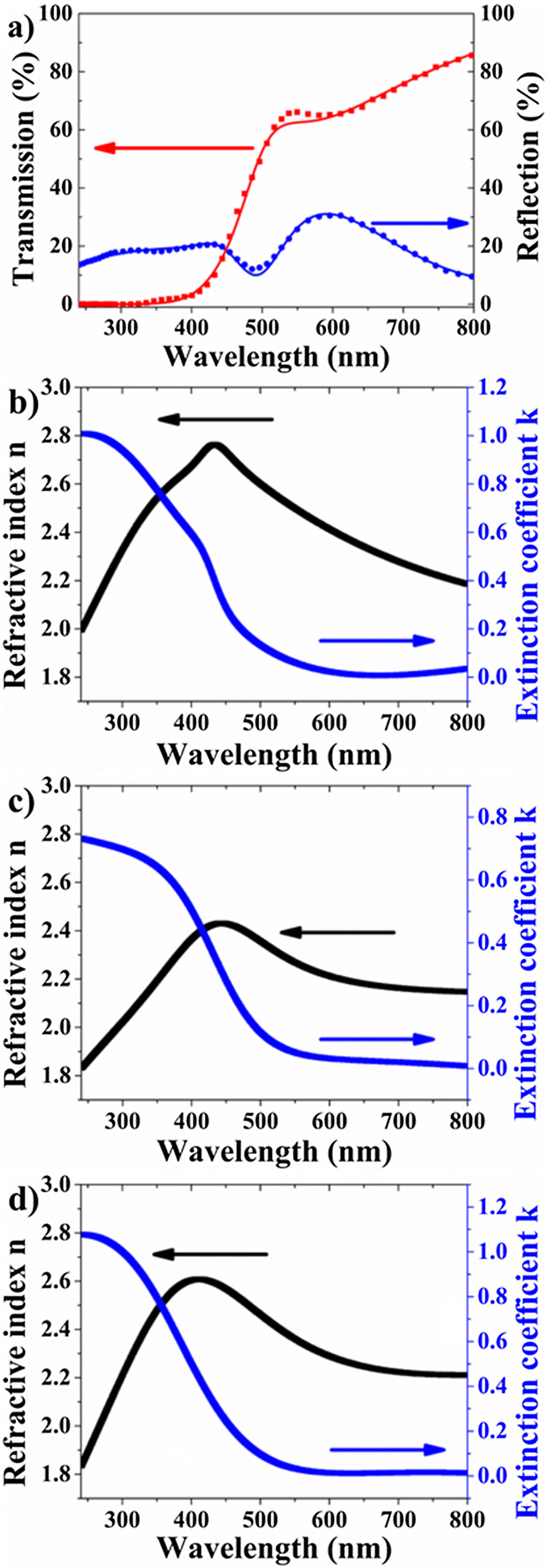
Optical analysisFig. 8a displays the optical transmission and reflection spectra of thin BiFeO3 thin film sintered for 60min (dotted line) and its adjustment using a three-medium SCI model (continuous line) in FilmWizzard software. There is a low transmittance in the near-ultraviolet region of the spectrum. A sustained increase in transmittance is observed in the spectral range from 420nm to 540nm. The transmittance of the BFO60 film has a linear increase between 550nm and 780nm, reaching values close to 85%. In the near-infrared region, the transmittance increases with the sintering time. All samples refractive index (n) and extinction coefficient (k) are shown in Fig. 8b–d. Peaks of the refractive index (2.43–2.8) appear between 400nm and 450nm, which likely corresponds to a transition in the direct energy band gap in the visible light region. There is an increase in the extinction coefficient for samples BFO30 and BFO60 at lower wavelengths; this may indicate the effect that sintering time and the presence of secondary phases have on light absorption. Therefore, it is possible to modify the optical constants of this material thin films by selecting an appropriate sintering time, which may be necessary when designing optoelectronic devices. There are sharp drops from 266nm to 600nm in k, and beyond 600nm is close to zero in all samples.
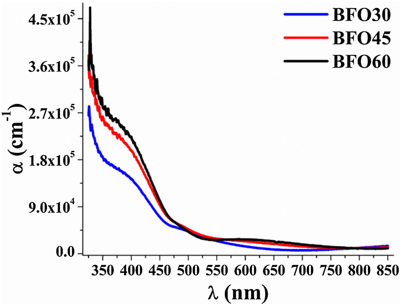
The thickness of all samples decreases as the sintering time increases. These were obtained by two methods: cross-sectional SEM images and UV–Vis Reflection-Transmission adjustment spectra. The thickness measured by a SEM image analyzer (Lince) was 191.5±13.83nm, 164.5±14.19nm, and 157.2±12.35nm for BFO30, BFO45, and BFO60, respectively. The thickness obtained by reflection-transmission adjustment spectra was 227nm, 183nm, and 112nm for BFO30, BFO45, and BFO60, respectively. The difference in thickness values obtained by SEM and by reflection-transmission spectra analysis is because in SEM images the thickness is obtained through the analysis of the cross section of the thin films, while by reflection-transmission spectra analysis it is obtained from models considering several aspects such as roughness. However, in both it is possible to observe the same tendency of thickness reduction with increasing sintering time. The analysis of the absorption coefficient spectrum of the films reveals the contribution of different absorption processes. Fig. 9 shows strong absorption in the ultraviolet region of the spectrum as a result of excitations through the fundamental band gap. The absorption coefficient value increases with the sintering time and the decrease in thickness. The 550–850nm region is the transparent area of the films regardless of their thickness. The absorption coefficient α(λ) of all thin films was calculated by the Eq. (1)[29]:
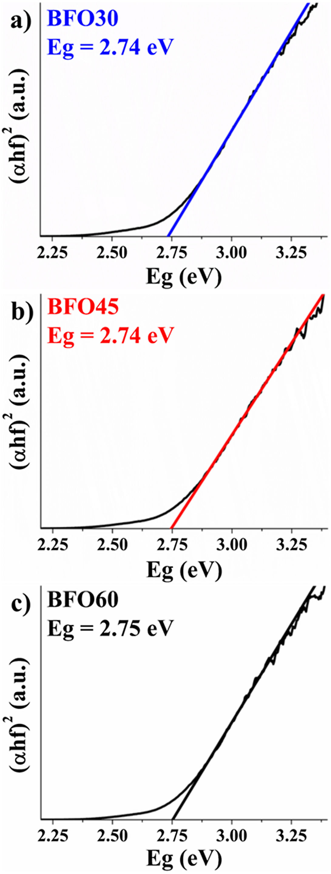
where T(λ) is the transmittance for a given wavelength λ and d is the film thickness.The absorption coefficient analysis as a function of photon energy at the fundamental absorption edge allows the determination of the optical band gap and the type of electronic transition. The optical band gap of the samples (Eg) was estimated using the Tauc method for allowed direct transitions [30]. Fig. 10a–c shows that the band gap value for all samples was 2.74–2.75eV. All films have a band gap within the visible spectrum, where the slight variations can be explained by discrete structural changes as is determined by Rietveld refinement. Thus, a Jahn–Teller type distortions in the FeO octahedron is observed via slight changes in Eg.
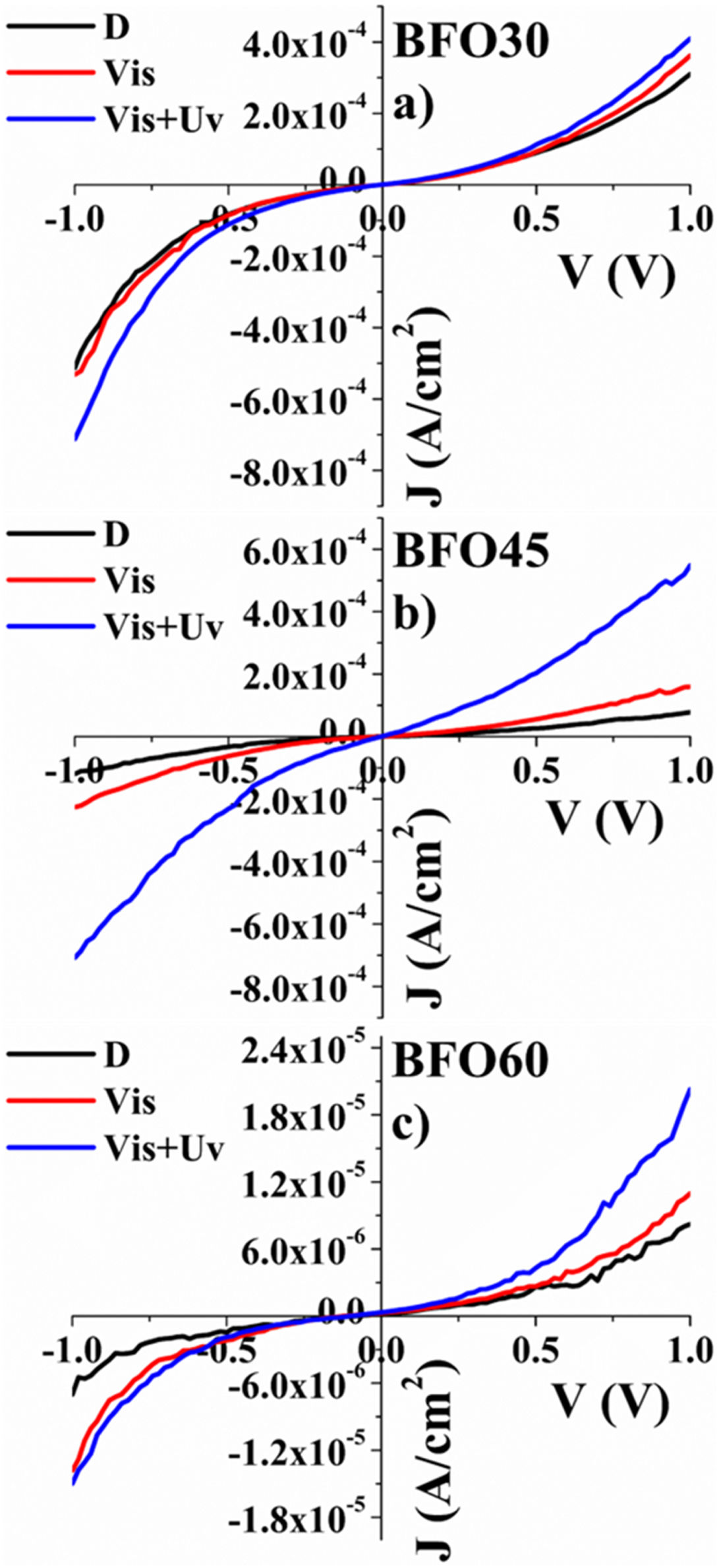
Photocurrent behaviorFig. 11a–c shows the current density (J)–voltage (V) graphs at room temperature of BFO thin films sintered at 550°C for 30, 45, and 60min (BFO30, BFO45, and BFO60, respectively). The effect of sintering time, as well as the presence of the Bi2O2.33 phase, is observed. The presence of secondary phases yields a high concentration of oxygen vacancies, which promotes charge carriers [31]. A diode-like effect was obtained in samples BFO30 and BFO60 due to the Schottky barrier formed at the interface of the BFO film and the FTO substrate; this is a typical behavior in BiFeO3 based thin films [32,33]. The current density (J) decreases as sintering time increases, as seen for the sample BFO30 at 1V (2.97×10⁻⁴A/cm2) and BFO60 at 1V (2.02×10⁻⁵A/cm2). It is also shown in Fig. 11 the current behavior under no illumination (Dark or D), visible light (Vis), and visible light with ultraviolet light (Vis+UV) using two lamps on all BFO films. All samples exhibit a photoconductive behavior when subjected to both types of light (Vis and Vis+UV). This is due to the generation of charge carriers induced by illumination with an energy higher than the material's band gap. The generation of charge carriers through excitation with light is possible in BFO base films and, therefore, induces photocurrent [34]. All this is evidence that sintering time greatly affects the electrical and photocurrent properties of BFO thin films.
The results show that the films obtained by sputtering with different sintering times in ambient conditions, using a homemade ceramic target synthesized in our laboratory free of secondary phases, allow us to obtain films with the rhombohedral phase of BFO starting from 30min of thermal treatment. However, the secondary phase Bi2O2.3 appears in all thin films. The samples have a wide grain size distribution, with mean values close to 85nm and a standard deviation close to 25nm, such that the average grain size is within the error bar for all treatment times. Due to the columnar nature of grain growth through sputtering, roughness around 20nm is obtained. However, the results show apparent effects due to the sintering time, among which is densification, as seen in the reduction in thickness of the films. There is a tendency to decrease the roughness, and a better contrast is also observed in the reorientation of induced ferroelectric domains for the sample with longer sintering time. The absorption coefficient shows an increasing trend with sintering time. In the J–V curves, it can be observed that there is a decrease in the current density for the sample with longer thermal treatment time, which may be due to a decrease in the concentration of defects, promoting the ferroelectric properties and therefore improving the contrast observed in the induced ferroelectric domains. To improve the ferroelectric properties of BFO films, a synthesis and post-processing method that eliminates or appreciably reduces the presence of the secondary phase is desirable. In future work, this problem will be addressed by implementing control of the substrate temperature inside the chamber of growth. Alternatively, in the post-processing method, the films can be treated in an inert atmosphere or subjected to rapid thermal processing to avoid the formation of the secondary phase.
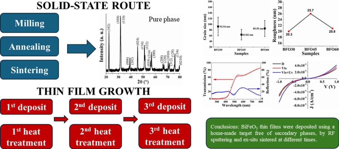
ConclusionsBiFeO3 thin films were deposited using a home-made target free of secondary phases, by RF sputtering and ex situ sintered at different times. A bismuth-rich secondary phase, changes in lattice parameters, phase percentage and crystallite size were identified in all films as increasing sintering time. The grain size was reduced from 92.54nm to 85.55nm for BFO30 and BFO60, respectively. Furthermore, grain size suppression was promoted by the presence of B2O2.33 as seen in BFO45. Raman spectroscopy allows us to corroborate the structural changes and the presence of the secondary phase as sintering time increases. The presence of the secondary phase proportionally influences the roughness of all films. Reorientation and observation of ferroelectric domains through PFM in all samples were performed. The Δθ increased as sintering time increased and thickness decreased. The elucidation of n and k spectra allows us to determine the effect of sintering time on the optical properties of BFO thin films. The band gap remained between 2.74eV and 2.75eV because the structural changes did not sufficiently affect the Jahn–Teller octahedron in the FeO octahedron. A diode-like effect was observed in BFO30 and BFO60 films, and a photocurrent was observed in all samples. Sintering time has various effects on the physical properties of BiFeO3 thin films, so it is essential to consider this factor for an adequate design of optoelectronic devices composed of this material.
To Autonomous University of Sinaloa, Faculty of Engineering Mochis. Center for research and advanced studies-IPN (CINVESTAV-QRO). To all CINVESTAV auxiliary personnel; M.C. Rivelino Flores Farias, Q. in A. Martin Adelaido Hernandez Landaverde, Agustin Galindo Sifuentes, Ing. Carlos Alberto Avila Herrera, Joaquín Gerardo Raboño Borbolla, Ing. Jose Eleazar Urbina Alvarez and IBT. Liliana Naranjo Naranjo. To Dr. Rafael Ramirez Bon for his support in optical measurements and use of FilmWizard software. This work was supported by the National Council of Science and Technology through the program 003615 – Doctorate in engineering sciences and The CONACyT project CB-2015 No. 255626.


