


A microstructure based on plate-like grains is expected in the obtaining of Bi4Ti3O12 ferroelectric ceramics, promoted by the Aurivillius crystalline structure that this material exhibit. This grain morphology would lead to conductivity making the functional response unpractical. In this frame, we address the control of the crystal growth which leads to this grain morphology by combining the effect of a simple thin film obtaining procedure with doping strategies. On the one hand, an aqueous solution-gel plus spin-coating methodology is performed here for the obtaining of these thin films. On the other hand, a simultaneous incorporation of Nd3+ and Nb5+ in the crystal lattice replacing Bi3+ and Ti4+, respectively, is conducted in this contribution. The results obtained by X-ray diffraction, UV–visible measurements and FESEM confirm that the incorporated dopants are able to block (or at least control) the mentioned crystal growth.
En la obtención de cerámicas ferroeléctricas basadas en Bi4Ti3O12 se espera una microestructura basada en granos en forma de placas, favorecida por la estructura cristalina de tipo Aurivillius que exhibe este material. Esta morfología de grano conduciría a una conductividad que haría que la respuesta funcional no fuera práctica. En este marco, abordamos el control del crecimiento cristalino que conduce a esta morfología de grano combinando el efecto de un procedimiento simple de obtención de lámina delgada con estrategias de dopado. Por un lado, para la obtención de estas láminas delgadas se lleva a cabo una metodología de disolución-gel en medio acuoso más spin-coating. Por otro lado, en esta contribución se lleva a cabo una incorporación simultánea de Nd3+ y Nb5+ a la red cristalina reemplazando cationes de Bi3+ y Ti4+, respectivamente. Los resultados obtenidos por difracción de rayos X, análisis por UV-visible y FESEM confirman que los dopantes incorporados son capaces de bloquear (o al menos controlar) el mencionado crecimiento cristalino.
The ferroelectricity of a ceramic material is quantified from the spontaneous polarization that the material exhibits and the coercive field. However, there is a strong anisotropy of the spontaneous polarization in Bi4Ti3O12 (BiT) ceramics. At room temperature, a spontaneous polarization in the ab plane of ∼50μC/cm2 has been measured, while a polarization of ∼4μC/cm2 in the perpendicular direction has been found, as well as a coercive field in ab of ∼50kV/cm and 7.8kV/cm in the c direction [1,2]. This anisotropy can be explained as a result of a double effect: the Aurivillius crystalline structure on the one hand, which consists on (Bi2O2)2+ layers located between layers with a perovskite-type structure [3–5], and the microstructure on the other. In fact, the first effect leads to second one. The Aurivillius structure promotes a plate-shaped grain morphology with the (Bi2O2)2+ layers parallel to their basal plane [6–9]. However, other reasons have been postulated to explain this plate-shaped grain growth. It can be ruled by the presence of a liquid phase rich in bismuth oxide formed during the sintering of BiT [10–13], since small local variation in the stoichiometry of the Bi2O3–TiO2 system could lead to its formation, as depicted in the corresponding phase diagram [14]. Furthermore, bismuth-based layered compounds present a relatively high electrical conductivity in the ab plane, which makes it difficult to polarize them and therefore the obtaining of a ferroelectric response. The anisotropy of this high electrical conductivity in BIT is such that the ratio between ab and c conductivity is of one order of magnitude at 500°C, presenting a mixed p-type ionic and electronic conduction. This conductivity could be also ruled by the mentioned typical microstructure, since there would be an exponential relation between the conductivity and the length/thickness ratio of those plate-like grains [15]. As a consequence, much of the research on BIT-based ceramics focuses on the decrease in their electrical conductivity, thus, blocking the growth of such plated-shaped grains by following several doping strategies [15–17]. Likewise, the processing method of obtaining a polycrystalline BIT seems to have a great influence in the conductive properties through the control of the growth of the grains in the form of a plate [11,18]. Besides, it is obtaining in the form of a thin film has aroused great interest for its integration into electro-optical devices. It could replace PZT in nonvolatile random-access memories (NVRAM) and dynamic random-access memories (DRAM) due to its relatively low dielectric constant, high Curie temperature, high spontaneous polarization (Ps) in the orientation of the c axis, and most importantly, for presenting good fatigue resistance [19]. In this frame, a combination of a novel processing methodology with two simultaneous doping strategies is proposed in this contribution. On the one hand, a simple aqueous solution-gel plus spin-coating method is used for the obtaining of Bi4Ti3O12 thin films, since this method has been successfully and recently used in the obtaining of similar bismuth-based thin films [20–22]. On the other hand, a simultaneous co-doping strategy is developed in this contribution, consisting in the incorporation of Nd3+ and Nb5+ in the crystal lattice replacing Bi3+ and Ti4+, respectively [23–25]. It has been described how lanthanide and Nb-substitution into their corresponding positions should reduce the conductivity at least one order of magnitude in bulk BiTi3O12 samples obtained by conventional method, due to the randomly microstructure induced by these dopants [2]. The same effect would be expected in a thin film geometry.
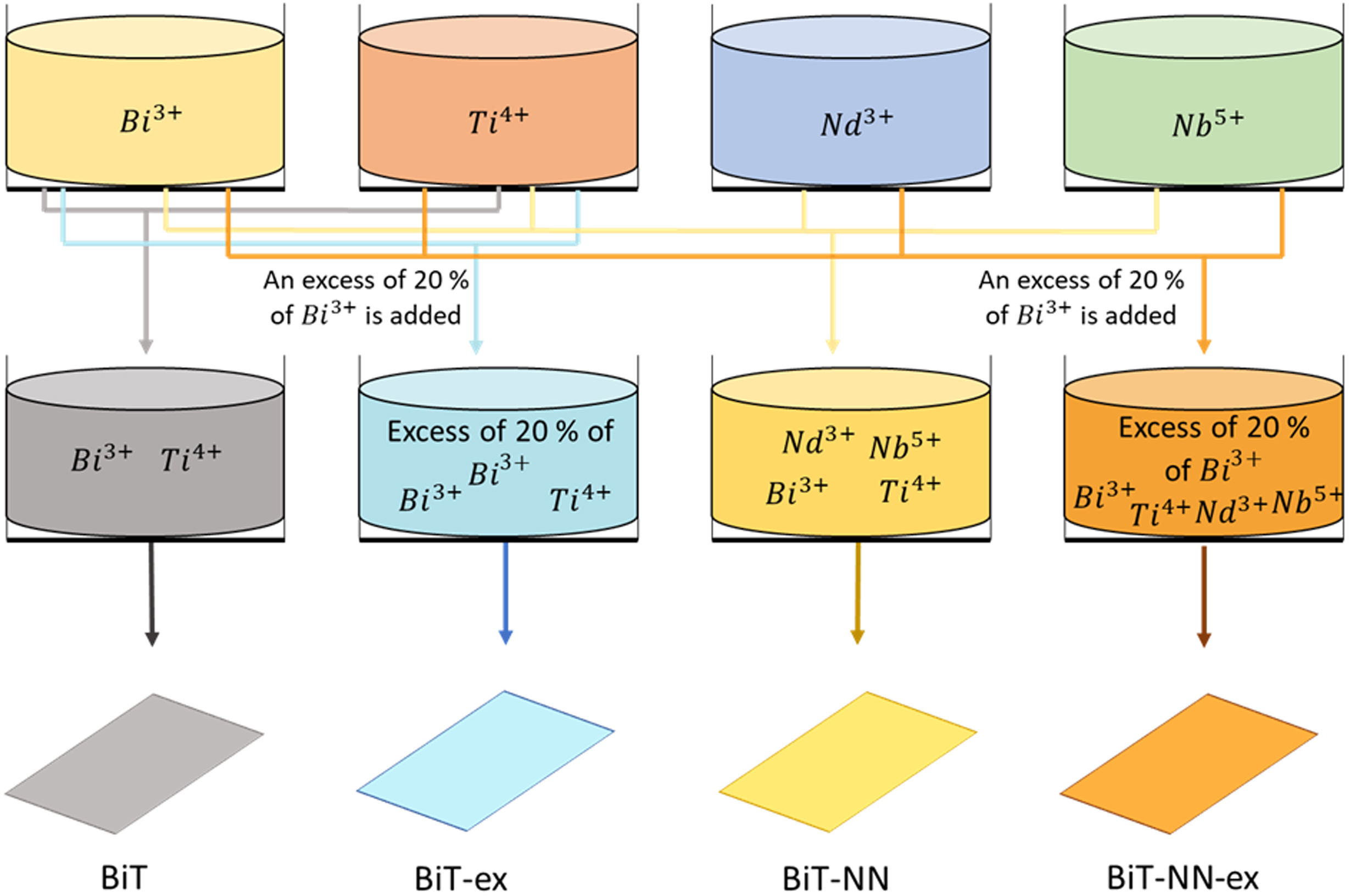
Experimental procedureAn aqueous solution-gel plus spin-coating procedure, which was firstly described by Van Bael et al. [26] is used in this contribution for the obtaining of two set of BiT thin films. A first set consisting on two non-doped BiT thin films, one containing an excess of 20% of bismuth, since this cation tends to volatilize, inducing a stoichiometric defect in bismuth that would lead to the formation of secondary phases [27–30]. In parallel, a second set consisting on two co-doped BiT thin film with Nd3+ and Nb5+, again one containing an excess of 20% of bismuth for the same purpose. To summarize this, the following nominal compositions were obtained: Bi4Ti3O12 (BiT), Bi4Ti3O12 with an excess of 20% of bismuth (BiT-ex), Bi3.2Nd0.8Ti2.97Nb0.03O12 (BiT-NN) and Bi3.2Nd0.8Ti2.97Nb0.03O12 with the mentioned excess of 20% of bismuth (BiT-NN-ex). For the obtaining of each specimen, firstly, the monometallic solution of Bi3+, Ti4+, Nd3+ and Nb5+ must be prepared by dissolution of each metal precursor in water: bismuth citrate for the first one, titanium isopropoxide for the second one, and the corresponding oxides for the Nd3+ and Nb5+ monometallic solutions. The monometallic bismuth solution requires the addition of ammonia, to increase the solubility of bismuth citrate [31], and ethanolamine to maintain the stability of the obtained solution. The Nd3+ monometallic solution also requires ammonia. However, the procedure to develop in the obtaining of the Ti4+ monometallic solution results quite different, since a water-soluble peroxocitrato-Ti (IV) complex must be obtained by an aqueous-chelated gel route [32,33]. For that purpose, a mixture of hydrogen peroxide and citric acid must be added to titanium hydroxide, which is previously obtained by the hydrolysis of titanium isopropoxide in water. Concerning the Nb5+ monometallic solution, the procedure is quite similar, requiring also the addition of ammonia, citric acid and hydrogen peroxide for the obtaining of a stable solution. Afterwards, these monometallic solutions are combined in stoichiometric proportions in order to obtain each multimetallic solution precursor of each thin film, as depicted in Fig. 1. On a second step of the process, each multimetallic solution is deposited onto a substrate with rotation by spin-coating. Simply apply two or three drops of the solution until the substrate is completely covered (dimensions of the substrate used: 1cm×1cm). Subsequently, the substrate is rotated with an acceleration of 1000rpm until a speed of 3000rpm is reached and this rotation is maintained for 30s. Then, the substrate rotation stops suddenly, without the need of a deceleration stage. Immediately after, three drying treatments are carried out for the removal of each mentioned solution component at 95°C, 200°C and 520°C during 1min. These temperatures were found after a thermogravimetric analysis carried out on the multimetallic solution containing Bi3+ and Ti4+. A loss of mass was found at those three temperatures, corresponding to the removal of the different components used in the obtaining of this solution [24]. These drying treatments are conducted on three hot plates arranged in series. After the first deposition, the sample is placed on the first plate at the mentioned temperature, removing it after 1min, and subsequently placing it into the next pre-heated plate. Eight deposition steps, with the corresponding drying treatment, are performed in total [24]. The substrate used consists on a pretreated Pt(111)/Ti/SiO2/Si in an SPS solution, a mixture of sulfuric acid and hydrogen peroxide in order to create a hydrophilic surface [26]. Eventually, a crystallization treatment is performed at 600°C during 1h to consolidate the thin film on a pre-heated hot plate.

The specific concentration of the monometallic precursor solutions was measured by ICP-AES on a Perkin Elmer Optima 3000 machine. The phase composition of the produced films was studied by X-ray diffraction (XRD) on a Bruker D8 advance diffractometer. UV–vis diffuse reflectance spectroscopy (DRS UV-vis) was carried out on an Analytik-Jena Specord 200 plus spectrometer equipped with an integrating sphere. A systematic microstructural analysis was conducted by field emission scanning electron microscopy (FESEM) using a Hitachi S-4700 cold FESEM microscope. FESEM micrographs were acquired using the SE secondary electron detector, since there was no difference in the contrast using the BSE backscattered electron detector. An image analyzer (Leica) was used to make dimensional estimations directly from the FESEM micrographs.
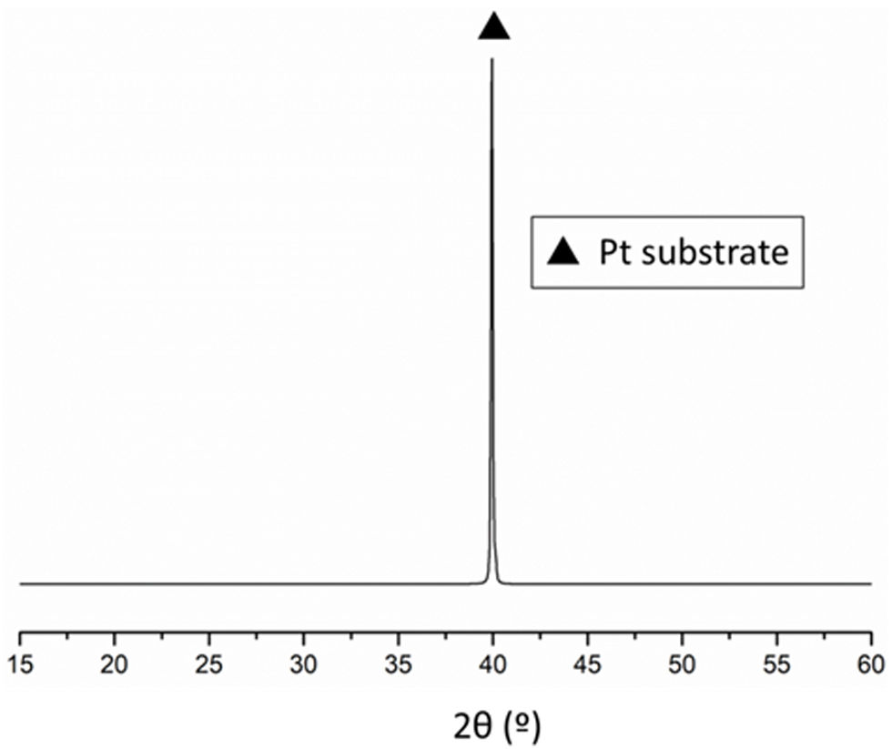
Results and discussionThe consolidated films were first analysed by standard Bragg-Brentano X-ray diffraction. In the diffractograms obtained in the analysis, only a single reflection is observed corresponding to the (111)-oriented platinum of the substrate, as depicted in Fig. 2. The reason can be found in the thickness of the substrate, much higher than the thickness of the film deposited on it. This diffractogram corresponds to the BiT thin film, but it can be considered a representative diffractogram, since the rest look similar.

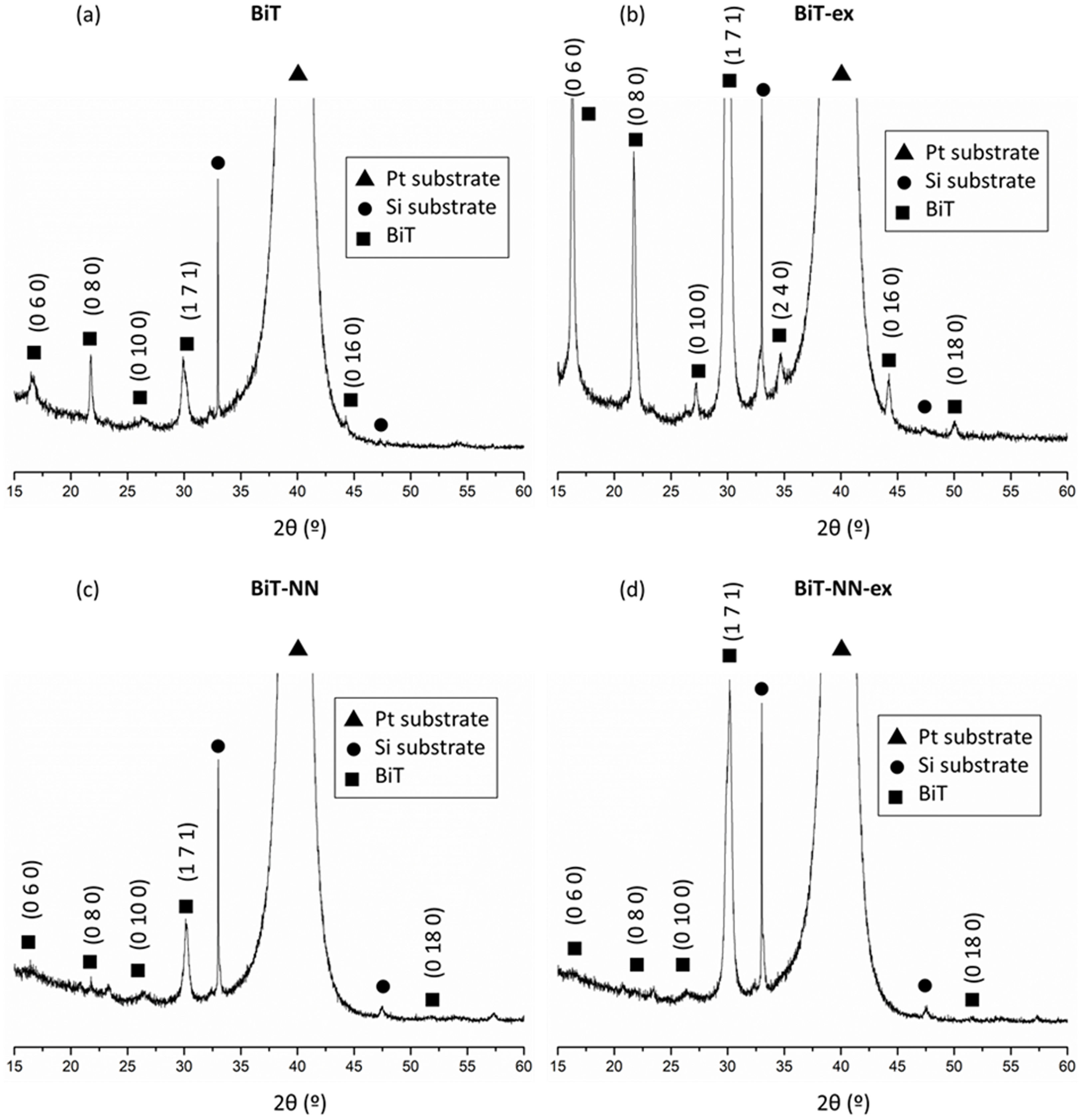
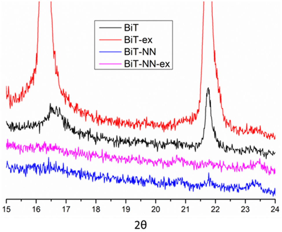
A magnification is required in order to find any other reflection hidden in the diffractogram noise (Fig. 3). All the reflections that accompany to the substrate correspond to the tetragonal structure of Bi4Ti3O2 (ICDD file no. 047-0398). Besides, diffraction maxima corresponding to the Si of the substrate are now visible with the mentioned magnification. No other phases rich in bismuth or iron are detected. However, the reflection maxima corresponding to the BiT phase have a different appearance in the four diffractograms. For the undoped film (BiT and BiT-ex), a higher intensity of the diffraction maxima is observed in the film containing an excess of bismuth oxide (BiT-ex), which seems to indicate that the material has evolved more during the heat treatment. The excess of bismuth probably leads to a transitory liquid phase and, as it has been mentioned above, it could accelerate the crystallization of the BiT phase during the sintering treatment. Furthermore, in the two undoped samples, an increase in the intensity of all the diffraction maxima corresponding to the (010) family is observed, especially in the sample synthesised with excess bismuth oxide (BiT-ex), suggesting a preferential growth of crystals in the ab plane, following the typical crystal growth habit of the BIT. However, this behavior is not observed between the two doped films, with and without excess bismuth oxide (BiT-NN and BiT-NN-ex). In neither of the two doped films an increase in the intensity of the diffraction maxima corresponding to the (060), (080), (0100) and (0160) planes is observed, even being an excess of bismuth in one of the samples. Dopants would therefore be blocking crystal growth in the form of plates [6]. These results suggest that the BiT-ex sample would exhibit a microstructure formed by elongated grains, but not in BiT-NN-ex sample. In fact, the diffractogram maxima which exhibits a highest intensity in the BiT-NN-ex sample corresponds to the (171) plane, which should mean that no elongated crystals are present. Comparing the two doped films with the undoped ones, the most notable difference is the little relevance of the diffraction maxima corresponding to the (010) family (2θ=16.24° and 21.71°) as depicted in Fig. 4. The higher intensity of these peaks observed in the two undoped films is indicative of the greater growth of the BiT crystals in the ab plane. It is expected, therefore, that the BiT phase grains in the two undoped films would be more elongated (greater growth in the ab plane), especially in the film with excess bismuth oxide where the intensity of these peaks is the highest observed. This could indicate that dopants would be blocking the diffusion processes and as a consequence the grains would not grow as much as platelets.
 BiT, (b) BiT-ex, (c) BiT-NN and (d) BiT-NN-ex, observed with the same magnification. The filled triangle is assigned to the signal corresponding to the Pt of the substrate and filled square is assigned to the Bi4Ti3O12 phase.")
, BiT-ex (in red), BiT-NN (in blue) and BiT-NN-ex (in pink) between 2θ=15° and 24°.")
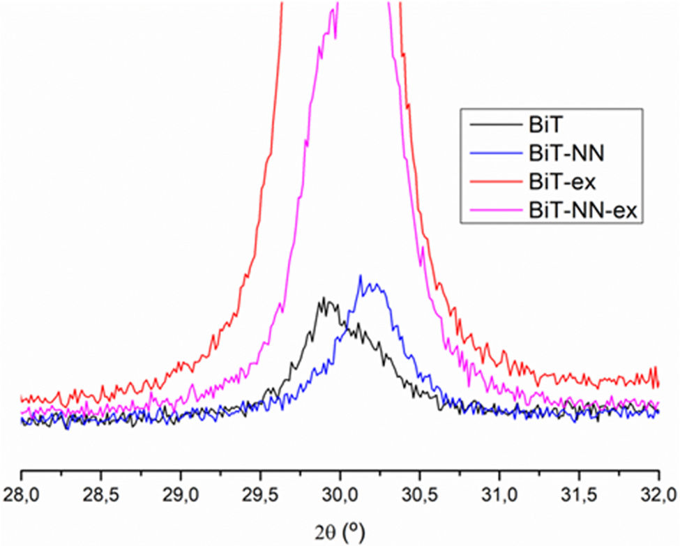
In the doped samples compared to the undoped ones, a shifting of the reflection maxima is observed, even in those samples containing an excess of bismuth (Fig. 5), thus suggesting the incorporation of the dopants into the Aurivillius crystal lattice of the BiT phase. The substitution of Nd3+ for Bi3+ in a position and the substitution of Nb5+ for Ti4+ in b positions modifies the crystalline structure due to the difference in radii of the cations [34]. The higher intensity observed in the samples containing an excess of bismuth can be ascribed to the higher crystallinity described before. The system has evolved more on these samples as a result of the formation of the mentioned transitory liquid phase during sintering treatment.
, BiT-NN (in blue), BiT-ex (in red) and BiT-NN-ex (in pink) between 2θ=28° and 32°.")
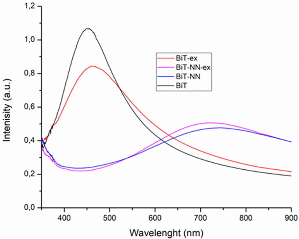
A series of UV–vis spectroscopy measurements were conducted to provide further information on how the electronic structure of BiT is modified upon doping, this being essential for elucidating the specific mechanisms governing the microstructural development of the low-temperature processed films. Fig. 6 shows the UV–visible absorption spectra of the non-doped and doped samples with and without bismuth excess. In our measurements, the BiT undoped film exhibits a band centred at 459nm. It can be ascribed to the transition from Bi 6s level into Ti 3d level [35,36]. This same absorption band are initially detected for the BiT (NN) doped compositions, although they are distinctly shifted from those of the undoped material; a red-shift is produced with the maximum of the band around 729nm, which is likely to result from the combined effect of dopant. The position of the transitions strongly depends on the Bi–O and Ti–O bond length and the site symmetry. This confirms or indicates the incorporation of the dopant into the structure since it produces an alteration of the structure. Also, it is observed that when the synthesis is carried with an excess of bismuth and the absence of doping, the intensity of the signals is lower than that of the sample without the Bi excess. This suggests probably the formation of a different phase of bismuth with no contribute to the absorption band.

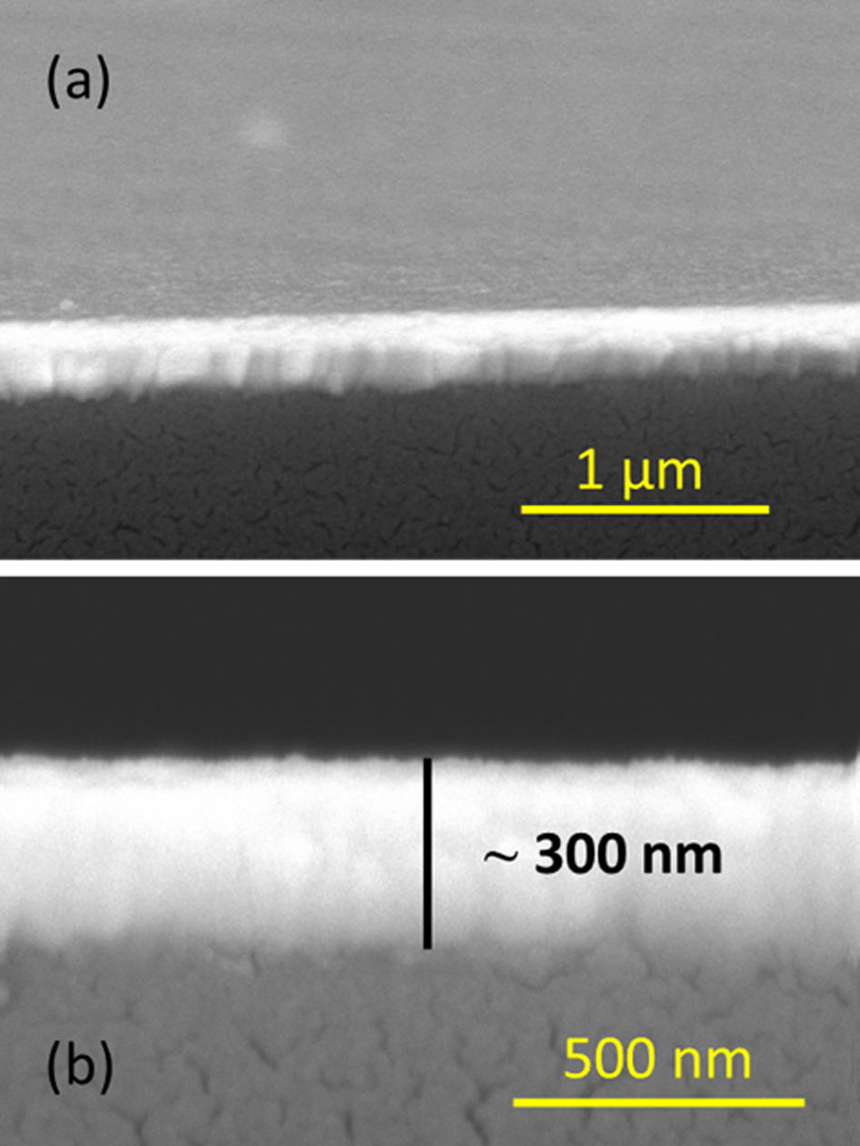
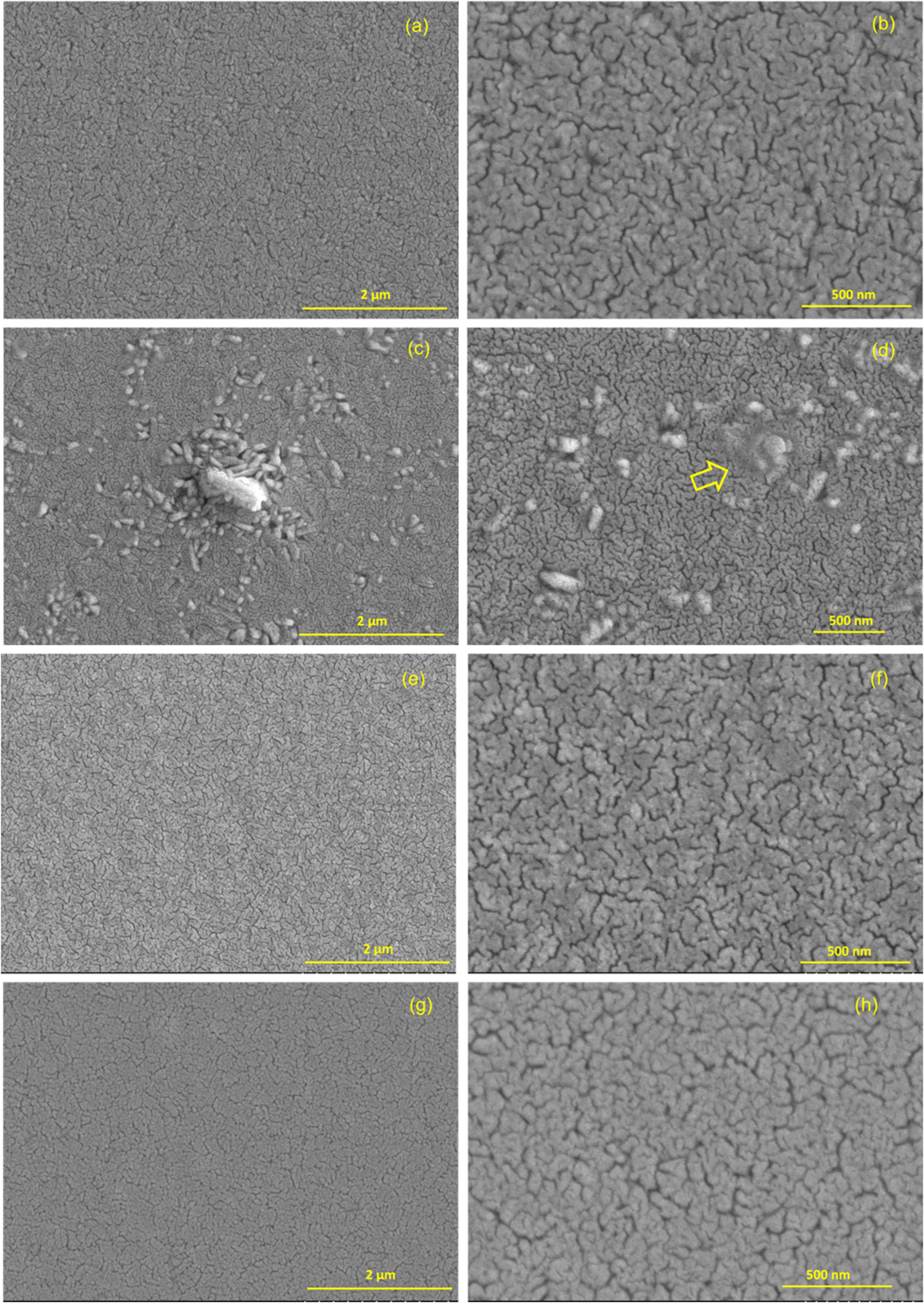
The microstructure of the films was next investigated by FESEM. This technique allows the obtaining of micrographs, both of the cross-sectional and the surface of each film. Fig. 7a shows the cross-sectional micrograph corresponding to the BiT sample as a representative way, since the rest of the samples look similar to this one, which demonstrates the reproducibility of the mentioned aqueous solution-gel plus spin-coating methodology for the obtaining of BiT-based thin films. As depicted, these micrographs were obtained with a certain degree of tilting in order to examine the uniformity of the surface. Homogeneous thin films, very well distributed throughout the entire substrate and exhibiting a high uniformity (in terms of morphology) were obtained by the mentioned thin film obtaining methodology in all samples. Nowhere is observed the presence of islands, nor agglomerated clusters, cracks or discontinuities. Eventually, any type of sizeable macroscopic defects, which are sometimes observed at the surface of polycrystalline films [37,38], are detected in these samples. Besides, an average thickness of ca. 300nm is measured for all the consolidated films, as depicted in Fig. 7b, where a representative micrograph corresponding to the BiT-NN sample is shown without the mentioned tilting. This thickness value is directly estimated from the FESEM micrographs using an Image Analyzer (Leica), after collecting up to more than 20 measurements per sample on different areas of the film. As can be deduced from this image, the individual layers constituting the films corresponding to the 8 depositions steps cannot be detected, and neither are any secondary phases observed, which is consistent with the X-ray diffractograms discussed above.
 BiT and (b) BiT-NN thin film samples.")
The top-view micrographs of the etched surfaces (Fig. 8) further give an indication of the uniform and crack-free surface texture. However, concerning secondary phases, we can find some differences between samples not observed in the cross-sectional micrographs neither in the DRX diffractograms. In the BiT thin film (undoped and without bismuth excess), which is depicted in Fig. 8a and b, grains which have grown close together and with a high degree of cohesion can be observed, since the sintering temperature of 600°C approaches to its melting temperature [39], thus it is likely that a liquid phase of bismuth oxide was produced during sintering, according to the results observed by XRD. This would have led to poorly defined grain boundaries in which a vitreous phase is present in some areas. In the undoped thin film containing bismuth excess (Fig. 8c and d), there is a visibly lack of homogeneity in some areas and the reason can be found in the presence of liquid bismuth oxide phase (sillenite phase) surrounding the BiT grains during the thermal treatment. In fact, in Fig. 8d, a non-defined area can be observed. It is precisely this liquid phase, thus creating a glassy area when it solidifies. The presence of this vitreous phase, not observed by XRD, is majority in the central area of the film. The lack of glass phase in the perimeter areas could be due to greater evaporation of bismuth oxide in these areas.
, BiT-ex (c and d), BiT-NN (e and f) and BiT-NN-ex (g and h). The amorphous phase, resulting from the liquid phase formed during sintering, has been highlighted with an arrow.")
In the micrographs corresponding to the BiT-NN film (Fig. 8e and f) a greater homogeneity is observed compared to the previous ones. The dopants block the growth of secondary phases and control the grain size. In fact, dopants decrease the diffusion mechanisms and increase the BiT melting point, which clearly differentiates it from the non-doped samples. Eventually, the doped sample containing an excess of bismuth, BiT-NN-ex, which is depicted in Fig. 8g and h, a similar scenario is observed in comparison to BiT-NN: a very homogeneous film containing round-shape grains. Again, this is a consequence of doping, which helps control grain growth and the appearance of secondary phases, even despite the presence of excess bismuth oxide in the material.
ConclusionsThin films based on the Bi4Ti3O12 system have been obtained by an aqueous solution-gel plus spin-coating methodology. The growth of plated-shaped grains is assumed in this system since the Aurivillius crystalline structure promotes this grain morphology. Consequently, this would lead to a high conductivity which would hide a hypothetical ferroelectric response. Here, we have overcome this issue by combining the effect of the thin film processing methodology with doping strategies. Comprehensive characterization of the main structural and microstructural features of the obtained films reveals that the incorporation of Nd3+and Nb5+ into the crystal lattice decreases the diffusion mechanism which rules the grain growth in the form of a plate. Besides, an amorphous phase, which is the result of a transitory liquid phase formed during the sintering treatment, is avoided when doping, leading to a higher degree of homogeneity and confirming that dopants increase the Bi4Ti3O12 melting point. As a consequence, rounded-shape grain microstructure has been reached in this contribution.
The authors acknowledge the Project TED2021-132779B-I00 funded by MICIU/AEI/10.13039/501100011033 and by the European Union NextGenerationEU/PRTR.