


In this paper we present the practical implementation of a high-speed polyphase sampling and demultiplexing architecture for optoelectronics analog-to-digital converters (OADCs). The architecture consists of a one-stage divide-by-eight decimator circuit where optically-triggered samplers are cascaded to sample an analog input signal, and demultiplex different phases of the sampled signal to yield low data rate for electronic quantization. Electrical-in to electrical-out data format is maintained through the sampling, demultiplexing and quantization processes of the architecture thereby avoiding the need for electrical-to-optical and optical-to-electrical signal conversions. We experimentally demonstrate a 10.24 giga samples per second (GS/s), 12-bit resolution OADC system comprising the optically-triggered sampling circuits integrated with commercial electronic quantizers. Measurements performed on the OADC yielded an effective bit resolution (ENOB) of 10.3 bits, spurious free dynamic range (SFDR) of -32 dB and signal-to-noise and distortion ratio (SNDR) of 63.7 dB.
En este artículo se presenta la implementación de una arquitectura de muestreo y demultiplexación polifásica para implementarse en convertidores analógico digitales optoelectrónicos de alta velocidad (OADCs). La arquitectura consta de circuitos muestreadores activados ópticamente conectados en cascada. La arquitectura muestrea una señal analógica y posteriormente demultiplexa diferentes muestras (canaliza) para reducir la velocidad de repetición de las mismas y así la cuantización pueda realizarse con circuitos electrónicos de baja velocidad. Una característica importante de esta arquitectura es que la señal analógica es conservada en el dominio eléctrico durante el proceso de muestreo, demultiplexación y cuantización, evitando la necesidad de los procesos de conversión de eléctrica a óptica y de óptica a eléctrica comúnmente usados en OADCs. Experimentalmente se implementó un sistema OADC de 10.24 giga muestras por segundo (GM/s) con 12 bits de resolución. Mediciones demuestran una resolución efectiva (ENOB) de 10.3 bits, rango dinámico libre de espurios (SFDR) de -32 dB, y señal a ruido y distorsión (SNDR) de 63.7 dB.
Digital signal processing (DSP) has revolutionized communication, radar and surveillance systems by offering unprecedented performance levels and adaptability. Further advancements in DSP now hinge on the development and progress of analog-to-digital converters (ADCs), which form an integral part of today’s DSP. Electronic ADCs are currently progressing at a rather slow pace; in contrast, optoelectronics ADCs hold the promise of providing great breakthroughs in the performance of the next-generation ADCs that can overcome the intrinsic limit imposed by conventional electronic platforms. Worthy of note are ADCs that employ optoelectronic technologies and optical signal processing concepts in their implementation because of their potential to achieve multi-gigabit/s sampling rates with high resolution. Recent progress in optical components has opened an unprecedented opportunity to develop practical optoelectronic ADCs. Several techniques for optical analog-to-digital converters have been reported [1, 2]. Among these are techniques that employ time-division multiplexing [3], diffractive optics [4], wavelength division multiplexing [5], soliton self-frequency shifts [6, 7], and optical pulse stretching [8].
A widely used optical ADC architecture employs electro-optic modulators in its sampling stage to convert and digitize electrical analog signal amplitudes into corresponding optical bit streams. Optical-to-electrical transducers are needed to reconvert optical samples into electrical signals in order that the quantization and coding functions be performed with electronic circuitry – as at present there are no practical, cost-effective optical quantizers available with performance that rival electronic quantizers. Intermediate demultiplexing stages may be required if the sampled data rate exceeds the processing speed of the electronic quantization and coding circuits. In this type of OADC architecture the nonlinear electrical–to-optical and optical-to-electrical transducers (modulator and photodiode) generate frequency spurious at the spectrum of the digital output signal. These generated frequency spurious decrease the SFDR and increase the total harmonic distortions (THD) that diminish the ADC bit resolution [9, 10, 11, 12]. Likewise, the time mismatch between the demultiplexed channels, due to nonlinear electro-optical components, creates bottlenecks that limit the sampling rate [13, 14, 15].
In this paper, we demonstrate a novel optoelectronics polyphase sampling and demultiplexing architecture integrated with electronic quantizers for the implementation of high-speed OADCs. A practical implementation of a 10.24 GS/s 12-bit resolution OADC system was developed. The complete and fully functional OADC consists of a) an optical network that generates a 10.24 GHz optical signal, used as a trigger source in the sampling process, and eight 1.28 GHz optical signals, used as a trigger clocks in the demultiplexing process, b) an optoelectronics network compose by a cascade connection of PIN photodiodes used to sample and demultiplex the RF analog signal, c) an electronic signal conditioning network, and d) 12-bits of resolution electronic quantizers used to generate the output digital codes. Measurements performed on the implemented OADC yielded an ENOB of 10.3 bits, SFDR of -32 dB, and SNDR of 63.7 dB.
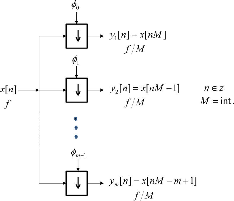
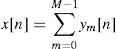
2Theoretical principleThe principle of the polyphase demultiplexing or decimating architecture is shown in Figure 1. An input time-sequence of samples x[n] with repetition rate f, is demultiplexed into m subsamples y1[n]=x[nM], y2[n]=x[nM−1],.,ym[n]=x[nM−m+1], each with repetition rate f/M. The term n is the discrete time index, and M is the number of demultiplexed branches; the output sequence ym[n] span the input sequence x[n]. Mathematically, the input-output relations of the decimation (demultiplexing) process is represented by Equation 1.

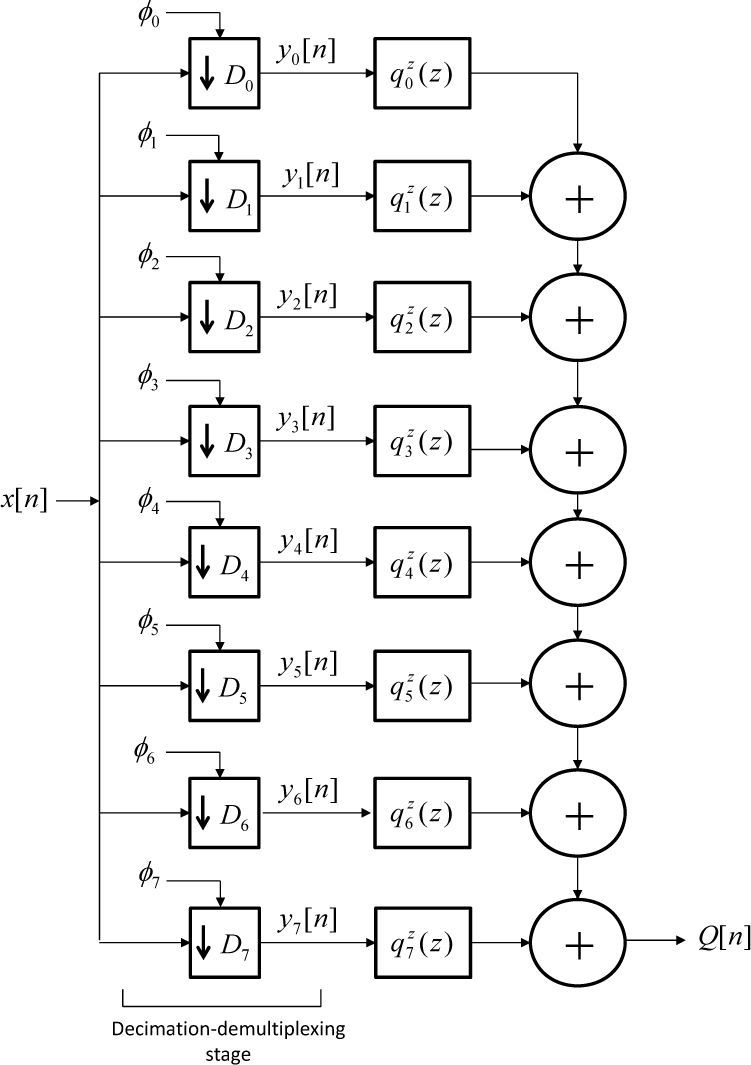
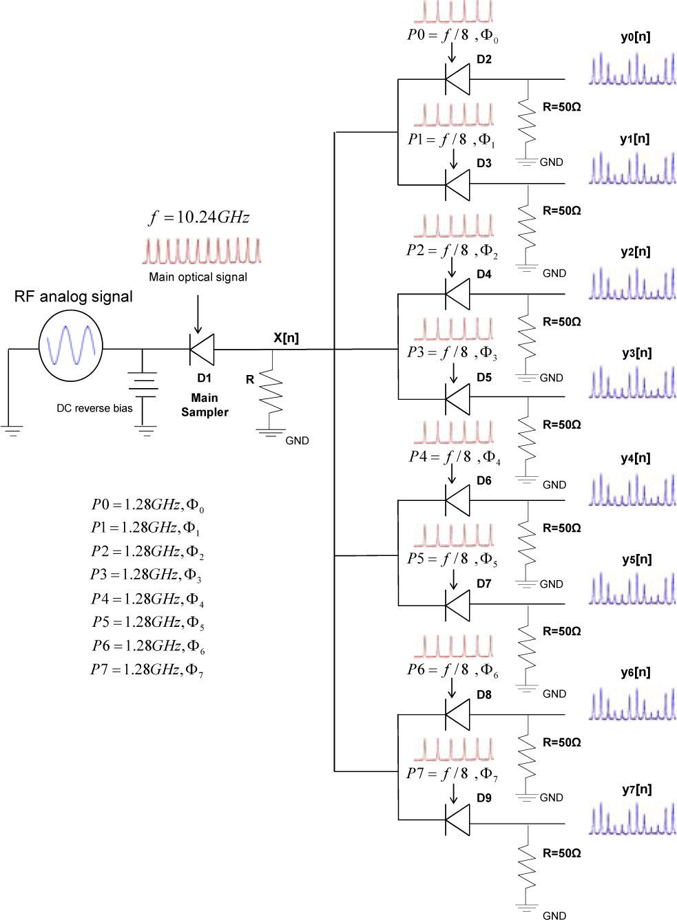
A block diagram of a polyphase processor using a decimation scheme for M=8 is shown in Figure 2. The diagram shows a one-stage divide-by-eight decimator where the sampled signal x[n] having repetition rate of f is demultiplexed (decimated) into eight subsamples, each subsample having a repetition rate of f /8. The decimation stage comprises the decimators from D0 to D7 which decimate by the factor M=8 different phases, from Φ0 to Φ7, of the input signal to generate the signals form y0[n] to y7[n]. Finally, the signals from form y0[n] to y7[n] are processed separately before being recombined to form the final aggregated digital signal Q[n].

In discrete-time domain, the output signal obtained using the polyphase processor is represented by Equation 2 where ymz(z) is the z-domain representation of the M-split and decimated branch signals, and qmz(z) represents the subsequent processing function implemented on each branch (In an ADC process, qmz(z) is the quantization function).
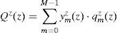
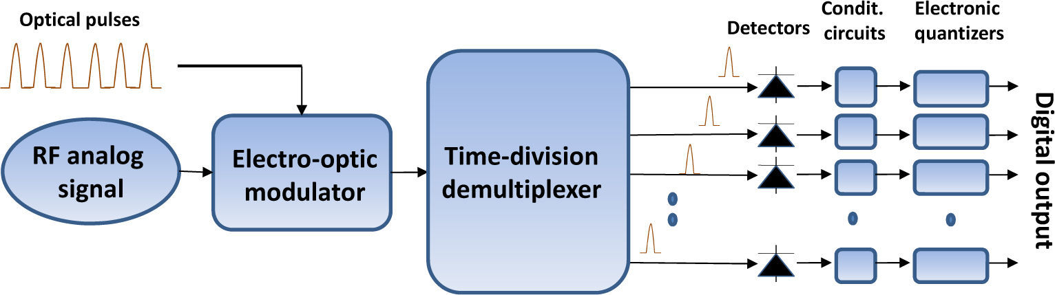
Figure 3 shows a schematic diagram of an optically-sampled OADC that utilizes a train of optical pulses to sample an electrical RF input signal applied to an electro-optic modulator. The resulting train of amplitude-modulated optical pulses can be detected, quantized and codified using electronic circuitry. In this kind of OADC, the sampling rate is limited by the speed with which the associated electronics can quantize and codify the detected optical pulses. An attractive means for increasing the sampling rate by a factor M is to use a 1:M demultiplexer at the output of the electro-optic modulator to direct sequential optical pulses to a parallel array of M electrical quatizers each operating at a quantization rate of fs /M where fs is the aggregate sampling rate. The demultiplexer directs the sequential optical pulses to the appropriate detector and electronic quatizer. The demultiplexing or decimating techniques require extremely precise match of all of the M parallel quantization channels so that digital outputs from these electronic quantizers can be interleaved to yield a precise representation of the analog signal sampled at fs.
3Practical implementation3.1Optical network
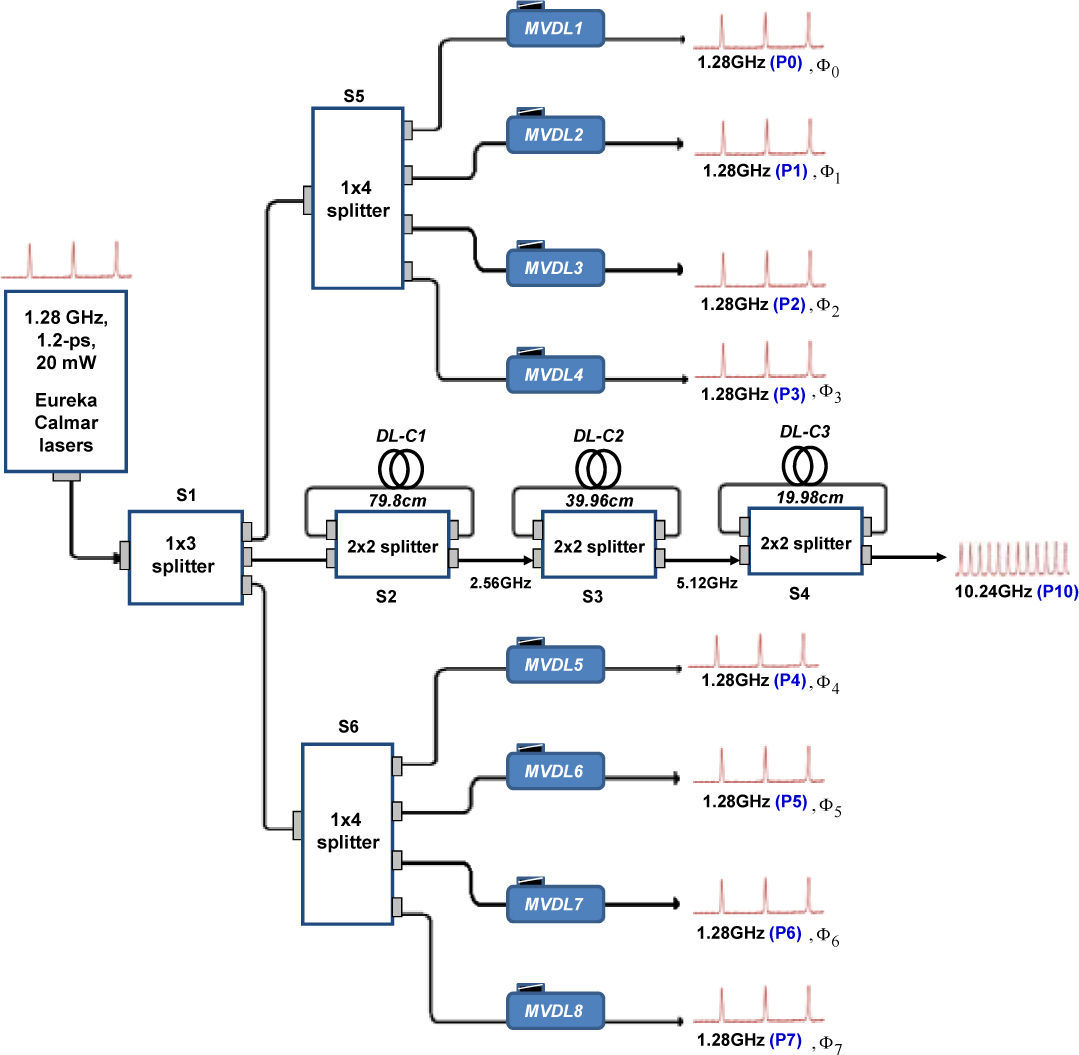
Figure 4 shows a schematic diagram of the optical network. The circuit was designed and implemented using passive optical components to generate a clock signal with optical pulse repetition rate of 10.24 GHz for RF sampling and eight clock signals with optical pulse repetition rate of 1.28 GHz for data demultiplexing. Manual variable optical delay lines (VLD-001-15-60) from General Photonics as well as single mode optical fiber (SM980G80) with corresponding group index of refraction of 1.466 at λ=1µm from Thorlabs was used to implement passive delay lines. The length of the optical fiber delay lines was calculated using the group delay equation, L=cT(λ)/N(λ), where c is the velocity of light, N(λ) is the corresponding group index, and T(λ) the desired group delay. A key feature of the circuit is that all clocks are generated from a single laser source (Eureka from Calmar lasers) with characteristics of optical pulse repetition rate of 1.28 GHz, optical pulse width of 1.2-ps, and optical output power of 20 mW. This ensures synchronize timing among all clocks without the need for an external control signal.

The clock signal of 10.24 GHz was generated by first splitting the main 1.28 GHz optical signal from the laser source into three using the 1x3 splitter S1, and then further feeding the signal emerging from the medial output port of S1 into a cascade connection of three frequency doubling optical circuits composed of 2x2 optical couplers [16, 17]. An output port of each of the three couplers is fed to an input port of the same coupler using a loop of optical fiber with specific length. As a result, the output repetition rate of each 2x2 coupler is doubled of the input frequency. In detail, the first 2x2 coupler, S2, has a feedback fiber loop of length DL-C1=79.8cm. This results in a frequency of 2.56 GHz at the output of S2. The optical feedback loop of the second 2x2 coupler, S3, has length of DL-C2=39.96cm. This doubles its frequency from 2.56 GHz to 5.12 GHz at the output. The optical feedback loop of the third 2x2 coupler, S4, has length of DL-C3= 19.98cm doubling the input frequency from 5.12 GHz to 10.24 GHz at the output.
The eight 1.28 GHz optical clocks were obtained by splitting the signals emerging from the upper and lower output ports of S1 into four using the 1x4 splitters S5 and S6 respectively. The eight 1.28 GHz optical clock signals are delayed relative to each other 12.20 ps by properly tuning the manual variable optical delay lines, from MVDL1 to MVDL8. The principal characteristics of the manual variable optical delay lines are operation wavelength 15-1550 nm, delay range 600 ps and insertion loss of±0.5 dB.
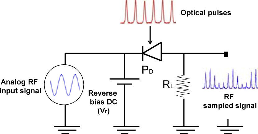
3.2Optoelectronic networkPreviously, a PIN-photodiode-based sampling and demultiplexing architecture was reported as an improvement over the drawbacks of electro-optic modulators based sampling schemes [17, 18]. A unique feature of this sampling and demultiplexing architecture is that electrical-in to electrical-out signal transfer is maintained for the optoelectronic sampling and demultiplexing circuits. In this work we are able to seamlessly integrate optical sampling and demultiplexing circuits with electronic quantization circuits without intermediary stages of electrical-to-optical or optical-to-electrical conversion. For ease of reference, we reproduce the basic optoelectronic sampling circuits as shown in Figure 5 in which the RF input signal (to be sampled) is connected in series with a reverse biased PIN PD and a load resistor. The PIN PD in the circuit acts as a fast normally-off optoelectronic switch whose ON/OFF states are actuated by optical pulses. In its OFF state, i.e. in the absence of an optical trigger, the PIN PD maintains high impedance causing an open current path in the series circuit arrangement with no voltage developed across the load resistor. On the other hand, in its ON state, i.e. when a laser pulse impinges on the PIN PD, its impedance is low allowing current through the circuit that results in a voltage across the load resistor. Thus when a stream of laser pulses, at a repetition rate f impinge on the PIN-photodiode, the amplitude of the input RF signal will accordingly be sampled at the same rate, with the sampled data appearing across the load.

Figure 6 shows a cascade connection of the sampling circuit with a one-stage divide-by-eight decimator. A 3 GHz bandwidth InGaAs PIN photodiode (PDT134X) from Hewlett-Packard was used to implement the sampling and decimation circuits. In operation, the analog RF sampled signal x[n] is distributed to all decimation branches. Each decimation branch is triggered by one of the 1.28 GHz optical clock. Since each decimation channel has been dedicated one of the eight optical clock outputs, and by virtue of the inherent channel-to-channel time-delay between the eight trigger clocks given by the passive delay lines, the onset of RF decimating would vary from channel-to-channel correspondingly. As a result, each channel decimates a different phase of the sampled RF signal. Thus effectively although the decimation rate of each channel is f / 8 the polyphase parallel decimation scheme network results in an aggregate rate of f *8.
3.3Electronic signal conditioning network and 12-bits electronic quantizers
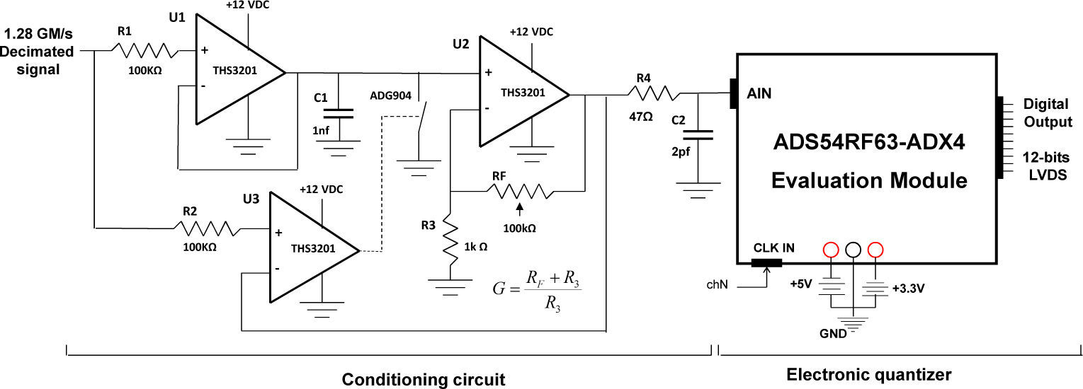
Each 1.28 GM/s output signal from the divide-by-eight decimator is electrically conditioned to meet the input voltage threshold of the electronic quantizers. Figure 7 shows a schematic diagram of the electronic conditioning and quantization circuit. The combination of the amplifier U1, U3 (THS3201) and capacitor C1 (1nf) works as a voltage-peak holder with auto reset. The circuit stretches each sample to meet the conversion time of subsequent electronic circuits. Attenuations generated in the holder circuit as well as offset mismatch are compensated by appropriately setting the gain of the amplifier U2 (THS3201). The RC circuit at the output of the operational amplifier U2 is to create an impedance match between the conditioning circuit output and the following electronic quantization circuit. Also, the RC circuit filters out spurious high frequency signals. This filtering process minimizes the correlated noise beyond the period of the decimated rate. The 12-bit electronic quantization circuit was implemented using the ADS54RF63-ADX4 evaluation module from Texas Instrument.
4Characterization results
To characterize the performance of the proposed OADC system, a 600 MHz sinusoidal signal with peak-to-peak amplitude of 310 mV from a 5520A Fluke calibrator was used as RF analog input signal. An oscilloscope display of the 10.24 GS/s sampled RF data stream is shown in Figure 8. The samples have peak-to-peak amplitude of around 300 mV as compared with 310 mV of the analog input signal. This reduction in peak-to-peak amplitude is attributed to the voltage drop in the PIN-PD of the sampling circuit. This voltage loss is compensated in the conditioning signal circuit by properly adjusting the gain of the amplifier U2.

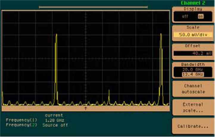
Figure 9 shows the first channel decimated signal corresponding to phase Φ0. The peak-to-peak amplitude of the decimated signals is around 285 mV as compared with 300 mV of the sampled input signal. This voltage reduction indicates electrical losses for the interconnection between the sampling and decimation circuits as well as the voltage drop in the PIN-PD of the decimation circuit. Also, this voltage loss is compensated in the signal conditioning circuit by properly adjusting the gain of the amplifier U2.
.")
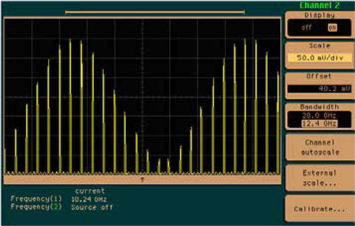
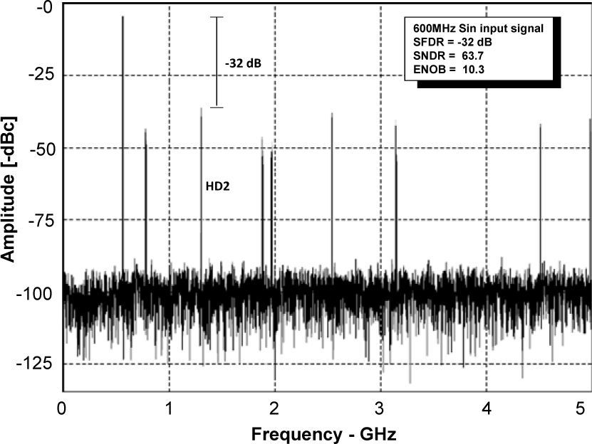
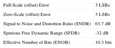
An Agilent U4154A logic analyzer system was used to transfer the digitalized signals from the quantizers of each decimation channel to a computer. Further after, the digitized signals of each decimation channel are aggregated to form the final digital representation of the analog input signal. We performed an FFT analysis with ‘Hamming’ windowing on 8192-point and 16 999-point acquisitions of the aggregated 10.24 GS/s digital signal. Figure 10 shows the resulting output spectrum and illustrates the dominant distortion tones. The plot spectral bandwidth is the Nyquist zone of the aggregated sampling rate. Spurious at different frequencies are observed. The spurious tone at 1.28 GHz, 2.56 GHz and 5.12 GHz are due to the offset mismatch effect (offset differences between channels). The spurious tones at 4.52 GHz, 3.16 GHz and 1.96 GHz, 1.88 GHz and 680 GHz are due to the combination of gain mismatch and timing errors effects between channels. The SFDR of the OADC converter was determined as the difference in dB between the value of the desired output signal (signal) and the value of the highest amplitude output frequency, HD2 (Highest Spur), that was not present in the input. Also, the signal-to-noise and distortion ratio (SNDR), and the effective number of bits (ENOB) were calculated using Equations 3 and 4 and summarized in Table 1 (where A is the amplitude of the frequency spectrum components).


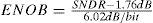
As a comparison of our proposed OADC system with other state-of-the-art OADC systems, in our approach we are implementing, from a single laser source, a multi-clock optical network using only passive optical components which do not introduce extra-jitter and eliminate the need of external synchronization and control signals [19, 21]. Thus, the phase noise due to the parallel multi-channel connection is reduced. Hence, the interleaved process becomes effective to reach a sampling rate of 10.24 GS/s with an effective resolution of 10.3 ENOB. Another unique feature of this approach compared with other all-optical ADC architectures [1, 21, 22, 23] is that the optically sampled RF signal always remains in the electrical domain and thus eliminates the need for electrical-to-optical and back to electrical conversions. In addition, no free-space optics is involved in the scheme, which makes the system more compact and stable with high potential for integration.
4ConclusionsWe have presented a practical implementation of a novel polyphase sampling and decimating architecture for photonics analog-to-digital converters. A 600 MHz RF input signal with peak-to-peak signal amplitude of 310 mV was used to characterize the designed OADC system. The architecture is based on a one-stage divide-by-eight decimator. The RF analog signal is sampled at 10.24 GS/s and further after decimated into eight channels at a rate of 1.28 GS/s by channel. Off-the-shelf electronic quantizers were then used to convert the decimated data into digital codes. The aggregated 10.24 GS/s digital signal was found to have an ENOB of 10.3 bits. The calculated SNDR was 63.7 dB, yielding a SFDR of -32 dB. The parallel processing of the sampled and decimated signals allows our scheme to be easily scaled up just by increasing the number of parallel processors. The scaling is accomplished without any increase in the speed of the components involved. Finally, our architecture allows for seamless and direct integration with electronic quantization circuits to achieve high-speed high-bit resolution analog-to-digital converters.