The obtaining of BiFeO3 in the form of a thin film represents a critical issue for its application in electronic devices since this is the required geometry for the integration of this material in microelectronic circuits. There are several techniques for this purpose, from those that use a gas or plasma phase to transport the precursors to the substrate, which would be included within the PVD or CVD techniques (for its acronym Physical Vapor Deposition and Chemical Vapor Deposition) to those that use a phase liquid for this transport, which would be included under the CSD (Chemical Vapor Deposition) techniques. However, among the large number of published papers, there is much controversy about which of them would be most suitable. It has been clearly demonstrated that all of them have the sufficient capacity to produce uniform and homogeneous thin films in thickness throughout the entire substrate, and although in many articles pure BiFeO3 films have been obtained with an exploitable functional response, others have reported the typical drawbacks that usually entails the obtaining this material: appearance of secondary phases, high leakages or a poor functional response. Nevertheless, there is a common aspect in the specialized literature that seems to be in agreement: the first group of techniques require very sophisticated equipment that involves high energy consumption in terms of temperature and pressure (vaccum), while the techniques that are based on solutions are characterized by their higher simplicity. In this context, the purpose of the present review is to summarize the main aspects of each technique in the obtaining of BiFeO3 thin films, from those that are more sophisticated to the simplest and environmentally benevolent ones, in order to provide an easier understanding of them.
La obtención de BiFeO3 en forma de lámina delgada representa una cuestión crítica para su aplicación en dispositivos electrónicos ya que es la geometría requerida para la integración de este material en circuitos microelectrónicos. Existen varias técnicas para este fin, desde las que utilizan una fase gaseosa o plasmática para transportar los precursores al sustrato, que se englobarían dentro de las técnicas PVD o CVD (por sus siglas en inglés de Physical Vapor Deposition y Chemical Vapor Deposition) hasta las que utilizan una fase líquida para este transporte, que se englobarían dentro de las técnicas CSD (Chemical Vapor Deposition). Sin embargo, entre el gran número de trabajos publicados, hay mucha controversia sobre cuál de ellas sería la más adecuada. Se ha demostrado claramente que todas ellas tienen la capacidad suficiente para producir películas delgadas uniformes y homogéneas en espesor a lo largo de todo el sustrato, y aunque en muchos artículos se han obtenido películas puras de BiFeO3 con una respuesta funcional aprovechable, otros han reportado los típicos inconvenientes que suele conllevar la obtención de este material: aparición de fases secundarias, corrientes de fuga altas o una pobre respuesta funcional. Sin embargo, hay un aspecto común en la literatura especializada que parece coincidir: el primer grupo de técnicas requiere de equipos muy sofisticados que implican un consumo energético alto en términos de temperatura y presión (vacío), mientras que las técnicas que se basan en disoluciones se caracterizan por su mayor simplicidad. En este contexto, el propósito de la presente revisión es resumir los principales aspectos de cada técnica en la obtención de películas delgadas de BiFeO3, desde las más sofisticadas hasta las más sencillas y respetuosas con el medio ambiente, con el fin de facilitar su comprensión.
It is well known that BiFeO3 single-phase ceramics have been one of the most investigated materials due to their promising multiferroic properties that could be exploited at room temperature. However, several drawbacks associated to the obtaining of an (almost) pure material with a practical response make it difficult to achieve. Specifically, three main drawbacks should be taken into account. The first one would be related to its metastability, since it has been proposed that the BiFeO3 perovskite phase is metastable with regards to the co-existent Bi2Fe4O9 mullite-type secondary phase and Bi25FeO39 silenite-type secondary phase [1–3]. The second drawback would be associated to the existence of a spin canting in the BiFeO3 structure which results in a weak magnetic moment in its unit cell according with Dzyaloshinskii-Moriya interaction. Moreover, this net magnetic moment exhibits a long-range superstructure consisting on a spin cycloid with a 64-nm wavelength that is incommensurable with the crystallographic structure [4–6]. The result is that, for single-crystals with size fairly larger than the spin cycloid, the net magnetization is zero, which at first, prevents a magnetoelectric effect. The third drawback would be ascribed with a poor electric response, including a low remanent polarization, high coercive field, low permittivity (dielectric constant) or low piezoelectric coefficients [7–11]. Nevertheless, it is the high leakages current that it usually exhibits the most remarkable problem, since it represents a serious impediment to its explotation in possible practical applications [7,8,12]. This high conductivity makes its polarization impossible and therefore prevents their use as a ferroelectric material. The cycles commonly described in the literature for BiFeO3 materials, although apparently they can show a high remanent polarization, have a rounded shape [13–16], which is characteristic of materials with high electrical conductivity and therefore provide very little information on the ferroelectric contribution. However, several satisfactory results have been obtained (in terms of blocking the growth of secondary phases and reaching a profitable practical response) for bulk BiFeO3 samples upon doping strategies ruled by a temperature-dependent kinetic mechanism, leading to a very narrow stability window in terms of processing temperature and time [17,18]. Despite the high interest in bulk samples of this material, which has been verified in the numerous articles published over so many years, the past recent years have redirected efforts to a thin film configuration, since certainly, from the point of view of applications, the utilization of film-based arrangements can be more realistic when it comes to miniaturization and integration into microelectronic circuits for data storage, sensors, spintronics, or visible-light photovoltaic devices [19–24].
Multiferroic BiFeO3 thin filmsThe interest in the obtaining of BiFeO3 thin films has triggered stimulating research during the past decade, which has involved several range of BiFeO3 doped compositions and what is even more arduous, the assessment of new methodologies of diverse complexity [25–30]. Certainly, as mentioned above, from the point of view of applications, the utilization of film-based arrangements can be more realistic when it comes to miniaturization and integration into microelectronic circuits for data storage, sensors, spintronics, or visible-light photovoltaic devices [19–21]. One has to go back to 1986 to find the first article published in which a BiFeO3 thin film has been obtained [31]. It was fabricated by RF sputtering, which is based on the transportation of a BiFeO3 vapor phase from the target to the substrate, and its corresponding electrical and magnetic response is discussed. It was not until 1991 when we can find another article dealing with the obtaining of a BiFeO3 thin film, and actually, only four articles were published during the nineties [32–35], in which BiFeO3 thin films were obtained with similar techniques to sputtering such as Pulsed Laser Deposition. It is in the first decade of the 2000s when a general interest in obtaining BiFeO3 thin films started to increase exponentially, and it will be growing up to date. One of the main reason for this interest lies in the fact that most of those mentioned drawbacks exhibited by bulk BiFeO3, like its metastibility with regards to the co-existent Bi2Fe4O9 and Bi25FeO39 secondary phases [2,3,36], its demonstrated high leakage currents leading to a deprived electrical behaviour [8–10,15,16] and even a (sometimes) unsatisfactory magnetic performance due to the exhibited espiral magnetic ordering [4–6], may be solved upon producing the material in the film geometry [8,37–40]. In a recent review by D. C. Arnold [8], it is concluded that the low remanent polarization exhibited by BiFeO3 bulk ceramics can be increased by several orders of magnitude when it is processed as a thin film sample; as the author methodically explains, calculations carried out by LSDA (Local-Spin Density Approximation) predict that BiFeO3 can reach remanent polarization values between 90 and 100μC/cm2, but, experimentally, values in this range are only achieved when the material has been produced as a thin film. However, there are many authors who contradict this statement, or at least they question whether the improvement of the properties is specifically due to the thin film configuration itself, and a serious controversy can be found among the large number of papers published on the subject. [8]. For example, in 2003 Wang et al. [37] published an article in which they claimed to improve the saturation magnetization and the remanent polarization values of BiFeO3 films by an order of magnitude, attributing this improvement to the stress that is generated by the lack of physical coupling between the thin film and the substrate (“misfit strain”). On the contrary, Eerenstein et al. [41], suggested that the improvement in the multiferroic response of the material and particularly of its magnetic behaviour is not due to the thin film–substrate interaction, but to the presence of Fe2+ ions. In response to this comment, Wang and co-workers admitted the existence of these cations in the thin films [42], but they further suggested the possibility of a gradual increase in the angle of the edged spins with the reduction of the thickness of the thin film and, therefore, with the stress produced in the interaction with the substrate. Years later, in 2005, Bai et al. [38] published results in which they observed how the epitaxial restriction is capable of breaking the spin cycloid, leading to high magnetization with very small fields, and later, in 2009, Ryu et al. [39] endorsed the theory of Wang et al. [37] when observing how the saturation magnetization increased remarkably with the reduction of the thickness of the thin film and therefore with the “misfit strain”. More recently, authors such as Tang et al. [40] confirm again that with increasing thickness of the thin film, magnetization decreases, which would be in line with previous studies, although they also observed how dielectric properties, ferroelectric response and leakages improve with this increase in thickness. As far as the electrical response of the BiFeO3 thin films is concerned, saturated ferroelectric cycles are found in many published works [37,43,44] although on many occasions it has been observed how these are not very reproducible results, with a high disparity in the values of remaining polarization perhaps due to stress-stabilized structural modifications [37]. Furthermore, electrical conductivity problems are often also observed when working with BiFeO3 thin films [41,45–48]. Some authors attribute the origin of this high conductivity to the presence of secondary phases such as Bi2O3, Bi25FeO39 or γ-Fe2O3[46,47], while other authors assure that it is due to the defects structure, specifically the presence of oxygen vacancies and/or iron ions in +2 oxidation state [41,45].
According to what it has just been described here, the functional response seems to be dependent on the thickness with which the BiFeO3 films are fabricated, although finding the optimal thickness is still a source of discussion in the literature [40]. But in addition, other considerations must be taken into account when working on thin films, like the rapid volatilization of Bi3+, for example. This situation, which is not uncommon in bulk samples [49], can lead to a higher concentration of oxygen vacancies and eventually result in an increased conductivity [50], so it can become particularly challenging in the film geometry due to the implicit high surface-to-volume ratio. In line with this issue, Pavlovic et al. [51] have observed that the film thickness can strongly affect the stabilization of the BiFeO3 perovskite phase, giving rise to a high amount of secondary phases if the film is too thin. These authors work on obtaining BiFeO3 thin films by a solution method followed by a spin-coating deposition and they affirm that the presence of the Bi2Fe4O9 mullite-type phase is increased when dealing with films of very low thickness; the explanation they propose is the aforementioned high surface-volume ratio: the large exposed surface area implies that the bismuth oxide, which has high vapor pressure, can easily evaporate during heat treatment. Consequently, there would be a loss in stoichiometry (Bi deficiency) and this would induce the formation of the iron-rich phase (the one with a mullite-type structure). This can be a serious limitation for the use of these multiferroic compositions in the field of microelectronic circuitry, where film thicknesses in between a few hundred nanometres and fractions of nanometres are typically demanded; moreover, the impediment would come not only from the presence of the iron-rich secondary phase, but from strong interactions with the substrate: as reported also by Wang et al., the crystal structure of BiFeO3 can change from rhombohedral to orthorhombic in epitaxial thin films [37], with the corresponding modification in the functional properties. This actually makes the substrate selection a critical parameter in obtaining BiFeO3 in the form of thin films, since that interaction can also cause preferential orientation, stress or texturing. A widely used substrate is that constituted by Pt(111)/Ti/SiO2/Si [51,52] or Pt(100)/Ti/SiO2/Si [53], since they can favour the epitaxial growth. For the same reason, the use of substrates of Si(100) [54], SiO2(100) [55], SrTiO3(111) [39,56,57], Pt(111)/TiN/Si3N4/Si(100) [58] and/or Si substrates coated with LaNiO3[59,60] are also widely extended. Glass substrates and indium doped tin oxide (ITO) substrates have been also used [45]. A very novel practice which is currently being tested is the possibility to grow BiFeO3 thin films on flexible polymer substrates. The goal is to enable their incorporation into next-generation flexible electronics systems [61], which is one of the fastest growing technologies that our society is witnessing today [62–65]. The challenge is great, mainly because of the thermal incompatibility between the crystallization temperatures of the involved metal oxides (typically above 600°C) and the thermal stability of the flexible polymer substrates conventionally used (below 400°C). Even though, Bretos et al. recently achieved the growth of BiFeO3 thin films on flexible plastic substrates by a solution processing involving three different (but complementary) strategies to induce the crystallization of the perovskite phase at a lower temperature limit of 325°C [61]. This “three-in-one” approach is based on the synthesis of metal precursors with a molecular structure similar to the crystalline structure of the oxide phase, which additionally allows both photochemical and internal combustion reactions taking place in the thin films. The flexible BiFeO3 thin films obtained from a specifically designed molecular complex with N-methyldiethanolamine yield a large remnant polarization of 17.5μCcm−2, also showing photovoltaic and photocatalytic effects. This result paves the way for the direct integration of an interesting class of oxides with photoferroelectric properties in flexible devices with multiple applications in information and communication technology, and energy [61].
Finally, it is worth mentioning that the choice of the specific deposition route is in itself a key factor in defining the properties and final performance of the obtained thin films. The main characteristics of some of the processing methods that are or have been used to fabricate BiFeO3 thin films are detailed below and constitute the core of this review article. In doing so, one common way to classify these methods and processing approaches could be the one that takes into account the range of thicknesses obtained with each type of deposition technique. Depending on its value, we will be facing a thin or thick film production technique. For this reason, and as a generalized criterion, it is considered that for thickness values less than 1μm the technique will be included in a “thin film” procedure [66]. A more extended classification criterion is that based on the process that is carried out during the deposition method, thus existing purely physical or purely chemical techniques; there exists however a wide range of processes, such as those based on luminescent discharges or reactive sputtering, which involve a combination of both chemical and physical processes, so they should be rather considered as physical-chemical deposition methods [66]. Eventually, the most widely used classification, which will also be followed in this work, is the one that considers the aggregation state of the medium used to transport the BiFeO3 precursors (or the BiFeO3 itself) and deposit them on the substrate. This classification generates two main categories of deposition methods: those using a vapor (or plasma) phase and those using a liquid medium.
BiFeO3 thin film processing through deposition methods based on vapor (or plasma) phase transportationWithin the film deposition methods that use vapor (or plasma) medium to transport the perovskite phase precursors, there are two distinct types of processing techniques: Physical Vapor Deposition (PVD) and Chemical Vapor Deposition (CVD). The difference between them lies in the fact that in the first block of techniques it is BiFeO3 itself which is sublimated and subsequently transported from the source to the surface of the substrate, where it condenses forming a thin and solid film [66]. In the second block, reagents such as Fe2O3 and Bi2O3, or other iron and bismuth precursors of different complexity such as [CpFe(CO)2]2 and BiCl3[67], are evaporated and transported to the surface of the substrate where they react each other in gas phase. The approach is very similar to PVD, except that in this last case a chemical reaction occurs prior to deposition. Table 1 summarizes some of the main features of the BiFeO3-based films that can be produced with each of these processing methods.
Summary containing the main results obtained in the synthesis of BiFeO3 thin films by using each of the high energy consumption techniques based on vapor or plasma phase transportation.
| High energy consumption techniques (based on vapor or plasma phase transportation) | |||||
|---|---|---|---|---|---|
| Processing method | Film composition | Substrate | Film thickness | Functional properties | Ref. |
| PVD | |||||
| Sputtering | BiFeO3 | SrTiO3 substrate | ∼300nm | Ferroelectricity: 2r ∼64μC/cm2 | [70] |
| BiFeO3 | Si (100) substrate | – | Superparamagnetism due to secondary iron oxide phases | [74] | |
| Bi0.75Ba0.25Fe0.975Ni0.025O3 | Pt/TiO2/SiO2/Si | 180–290nm | Multiferroic:Ps ∼1μC/cm2Ms ∼40emu/cm3 | [75] | |
| BiFeO3 | p-type Si (100) | 300nm | Dielectric film exhibiting a stable insulation property | [76] | |
| BiFeO3 | Si Substrate | – | Optical film: high refractive index and low losses | [77] | |
| BiFeO3 | SrTiO3 substrate | – | Ferroelectrictty:2Pr ∼200μC/cm2 | [83] | |
| BiFeO3 | Pt/Ti/SiO2/Si(100) | 2μm | Ferroelectricity and piezoelectricity:Ps ∼152μC/cm2d33 ∼120 pm/V | [85] | |
| PLD | BiFeO3 | (111)-oriented SrTiO3 substrate | 30–200nm | Magnetic response:Ms ∼40emu/cm3 for 30nm thickness | [39] |
| Bi1−xEuxFeO3 | LaNiO3 coating Si(100) substrates | 324–419nm | Optical properties with refractive index and extinction coefficient of 2.25 and 0.04at 2eV | [59] | |
| BiFeO3 | Platinized silicon substrates | 150nm | Photoluminescence and ferroelectric domains patterns | [79] | |
| BiFeO3 | (110)-NdGaO3, DyScO3, GdScO3, NdScO3 and PrScO3 | 2–3nm | High piezoelectric response due to the presence of an MPB | [80] | |
| MBE | BiFeO3 | (111) SrTiO3 | 35nm | Magnetic response:Ms ∼0.04 and 0.03μB/Fe3+ | [81] |
| BiFeO3 | SrTiO3 coating Si(100) substrates | 40nm | G-type antiferromagnetic behaviour+and a residual ferromagnetism: Ms ∼180emu/cm3 | [82] | |
| BiFeO3 | (001) SrTiO3, (101) DyScO3, (011) DyScO3, (0001) AlGaN/GaN, and (0001) 6H-SiC single crystal substrates | 75nm | – | [92] | |
| CVD | |||||
| CVD | BiFeO3 | Glass substrates and Pt/SiO2/Si wafer | 320nm | Multiferroic behaviour with Ps ∼8.7μC/cm2, coercivity 135Oe and −115Oe, and Ms ∼8.9emu/cm3 | [67] |
| MOCVD | BiFeO3 | SrTiO3 substrates | Ultrathin film: 7–10nm | Ferroelectric switching behaviour | [93] |
| BiFeO3 | (001) SrTiO3 substrates | ∼30nm | Magnetic properties:Ms ∼70emu/cm3 and coercive field ∼130 Oe | [95] | |
| BiFeO3 | IrO2/Si substrates | ∼600nm | Piezoelectric properties confirmed by PFM | [96] | |
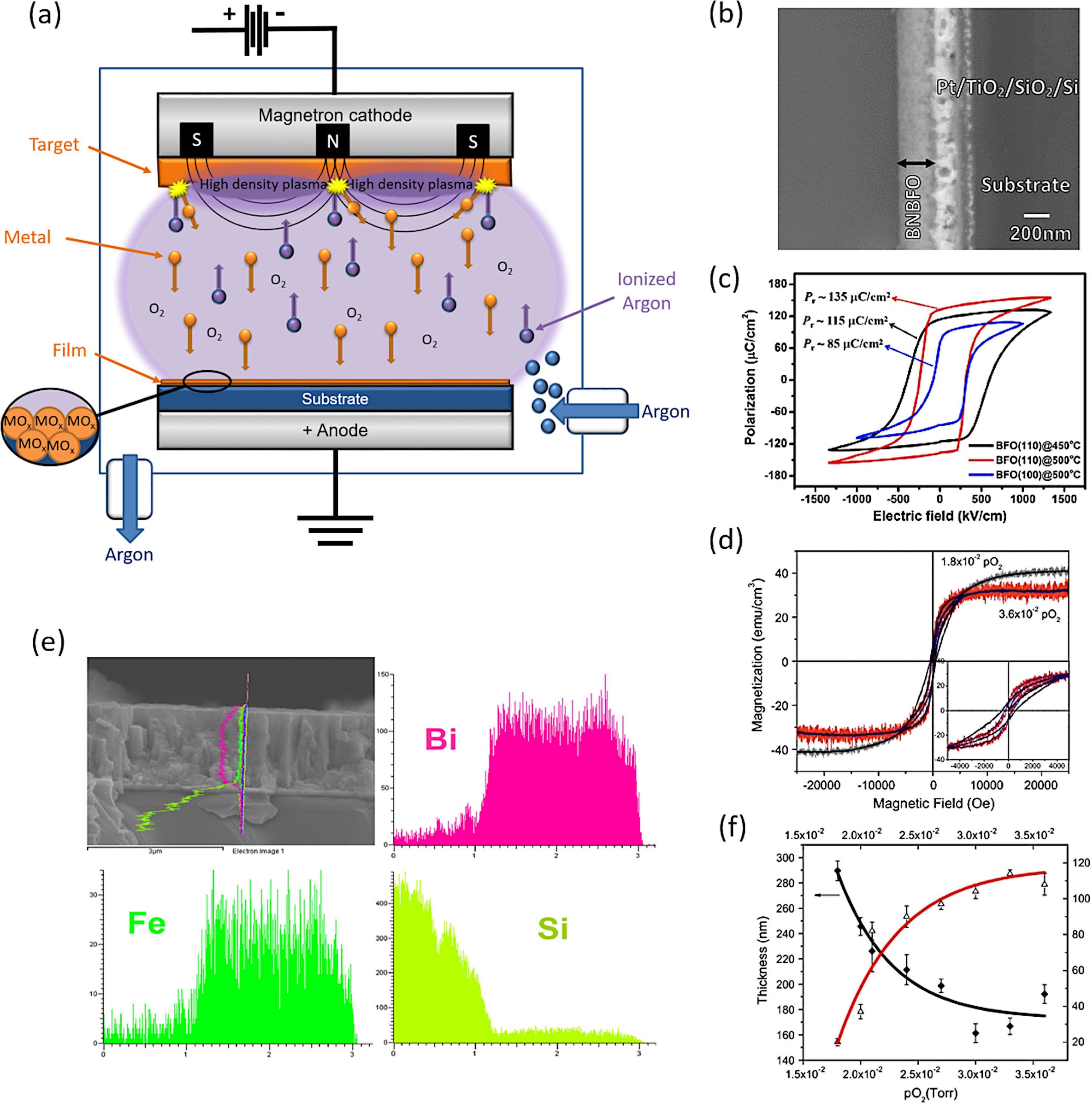
The PVD methodology encompasses different techniques that differ from each other in the mechanism they use to sublimate the material to be deposited on the substrate. Many of these techniques have been widely used to obtain BiFeO3 thin films during the past decade [68–90]. One of the most used would be the sputtering technique deposition. Actually, close to 200 articles can be found in the specialized literature for the obtaining of BiFeO3 thin films by using this technique. In this approach, BiFeO3 is previously sublimated by bombardment with highly energetic ions before being deposited on the substrate surface. This technique uses an ionized plasma which impacts against a BiFeO3 target, hitting the densely packed group of atoms and producing the subsequent expulsion of some of them from the surface. The expulsed atoms are then directed towards the substrate by the action of an electric field. These atoms, which are not in a state of equilibrium thermodynamic, condense on the substrate surface once they collide with it (Fig. 1a). The process takes place in a chamber where a high vacuum has been generated.
Sputtering for the obtaining of BiFeO3-base thin films. (a) Schematic representation of the mechanism that takes place during the formation of an oxide thin film by sputtering. (b) Bi0.75Ba0.25Fe0.975Ni0.025O3 thin film micrograph obtained by Scanning Electron Microscopy. Reproduced with permission. [75] Copyright 2016, Springer. (c) Ferroelectric hysteresis loop for a BiFeO3 thin film. Reproduced with permission. [85] Copyright 2020, Elsevier. (d) M–H curves for the Bi0.75Ba0.25Fe0.975Ni0.025O3 thin film. Reproduced with permission. [75] Copyright 2016, Springer. (e) BiFeO3 thin film with a profile obtained by EDS for bismuth, iron and the silica of the substrate. Reproduced with permission. [85] Copyright 2020, Elsevier. (f) Thickness decrease for a BiFeO3 thin film with the increase of O2 partial pressure. Reproduced with permission. [75] Copyright 2016, Springer.
This technique has provided very interesting results in the fabrication of BiFeO3 thin films. Rojas et al., for example, have recently succeeded in obtaining BiFeO3 thin films doped with barium and nickel (Fig. 1b, d and f), observing how an increase in the partial pressure of oxygen induces important morphological changes and a reduction of the film thickness (Fig. 1f) [75]. The films produced display an appreciable distortion of the rhombohedral symmetry but still they render an interesting and exploitable ferroelectric response. These authors actually used a processing variant known as RF sputtering, which is based on the alternation of the electric field in the vacuum chamber with the use of radio frequencies, in order to avoid the accumulation of charge on certain types of targets. Kaya and co-workers also employed RF sputtering to obtain BiFeO3 films with a thickness about 300nm and with optimal dielectric properties for use in capacitors with a certain range of applied voltages [76]. Another widely used sputtering variant is magnetron sputtering. In this alternative, a magnetic field is applied perpendicular to the electric field to increase the percentage of ions impacting the target (the electric discharge used in conventional sputtering is typically insufficient for this purpose). Some authors such as Somrani et al. [77] have used RF sputtering to attain BiFeO3 thin films free of secondary phases and with interesting optical properties, including a high refractive index and low losses, although the samples required a subsequent calcination at 700°C to consolidate the deposition. Moreover, the sputtering technique can also be used to obtain BiFeO3 thick films. In a recently published paper, H. Zhu et al. [85] have produced BiFeO3 films of around 2μm in thickness which exhibited a giant spontaneous polarization of around 150μC/cm2 (Fig. 1c and e); if confirmed, this would certainly be a relevant finding, specially since there is a widespread opinion that such a giant polarization can only be achieved in strain-induced tetragonal (-like) thin films up to a few hundred nanometers thick. However, it is important to mention that the technique has not always given such optimal results. Couture et al. [74], for example, have observed how after the sputtering deposition at room temperature and the subsequent calcination step, a BiFeO3 thin film is obtained with a high content of iron phases, such as magnetite and meghamite, which eventually lead to an unfavourable superparamagnetic behaviour and a low saturation magnetization.
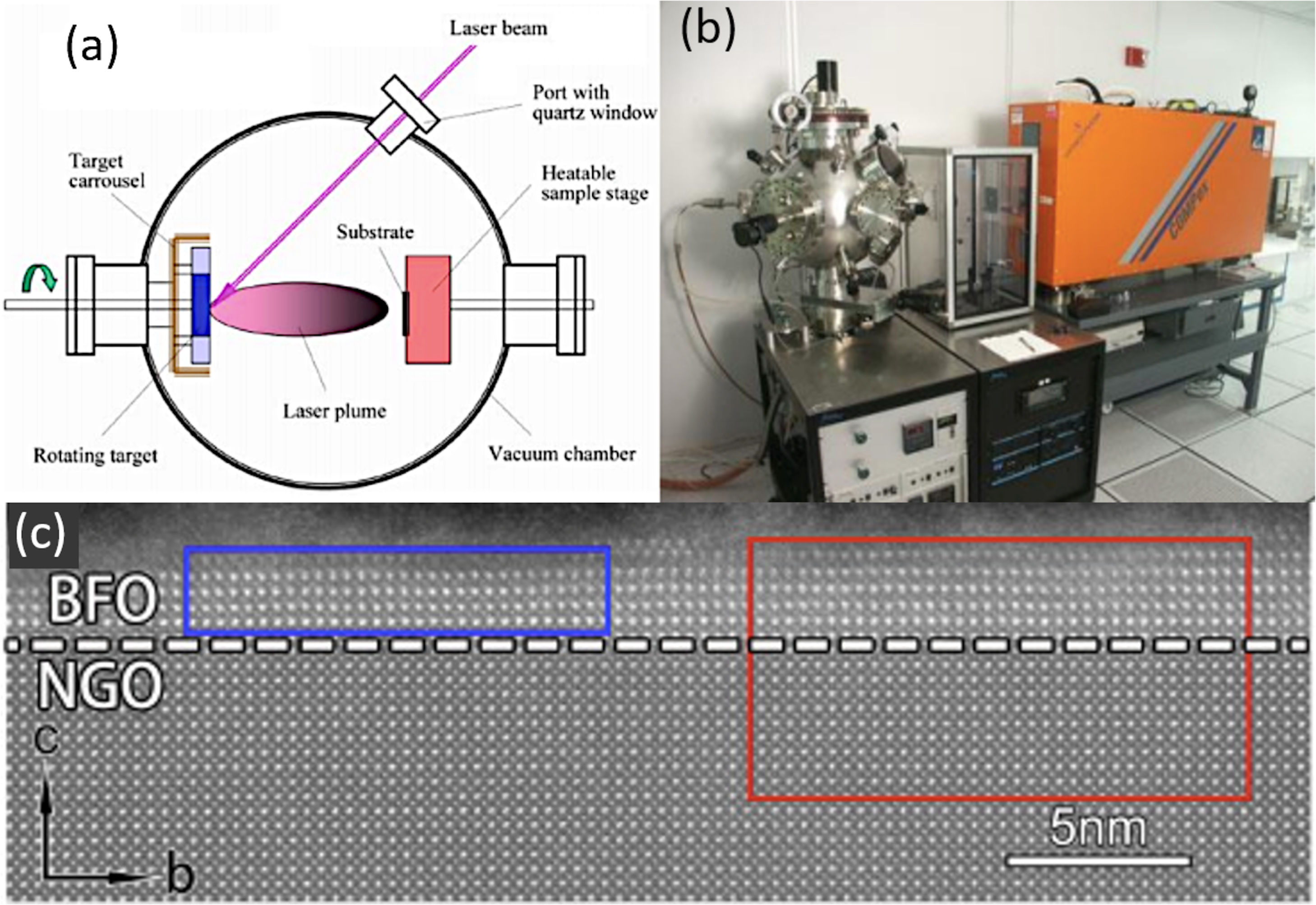
Another technique within the PVD grouping would be Pulsed Laser Deposition (PLD). In essence, the technique is very similar to sputtering, except that in this case it is a high power pulsed laser which impacts against the solid to sublimate it, producing a laser-target interaction (Fig. 2a and b). PLD also requires high vacuum and it has been widely used to obtain BiFeO3 films. Crassous et al. [78] used this processing methodology to produce La3+ doped-BiFeO3 films with thicknesses below 100nm, observing that there is a direct relationship between the arrangement of the ferroelectric domains and the film thickness. Similarly, Prashanthi et al. [79] obtained BiFeO3 films by PLD with photoluminescent characteristics (also noting the need for subsequent calcination), while Ryu et al. [39] found that the saturation magnetization of the film obtained by this PLD procedure increased with decreasing film thickness. More recently, Han et al. [80] have observed the formation of a morphotropic phase boundary (MPB) in BiFeO3 ultrathin films (just a few nm, as depicted in Fig. 2c) fabricated by PLD. According to these authors, the coexistence of the rhombohedral (R3c) and the orthorhombic (Pnma) phases of BiFeO3 is driven by an interfacial oxygen octahedral coupling which is exerted upon using different orthorrombic substrates. On the other hand, Knoche et al. [90], have observed a bulk photovoltaic effect in BiFeO3 thin films with stripe-domain pattern as the polarization of light is modulated from linear to elliptical to circular. This anomalous character allows the observation of a switch-like photovoltaic effect, i.e., ON and OFF state, by changing the helicity of circularly polarized light.
PLD for the obtaining of BiFeO3 thin films. (a, b) PLD equipment. Reproduced with permission. [91] Copyright 2020, Hampstead Psychological Associates. (c) Transmission Electron Microscopy micrograph for a BiFeO3 thin film obtained with 2–3nm of thickness on a (110)-NdGaO3 orthorrombic-perovskite oriented substrate by PLD. Reproduced with permission. [80] Copyright 2018, Elsevier.
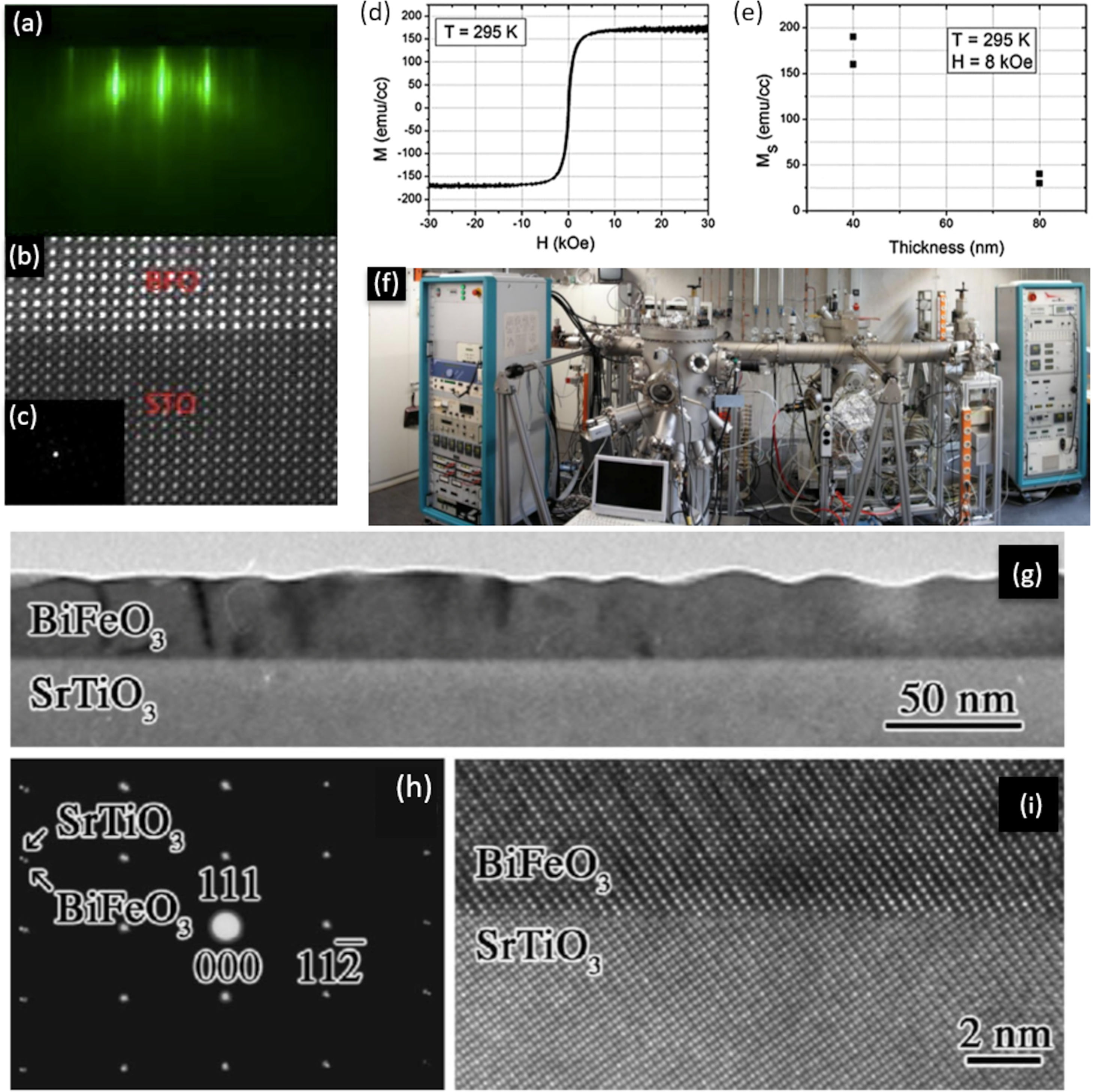
Another technique that does not involve a chemical reaction for the deposition of thin films (hence included among the PVD procedures) would be the Molecular Beam Epitaxy (MBE). Unlike the previous ones, in this process the solid is sublimated by the effect of temperature. When the conditions are suitable, the thin film grows reproducing the crystalline structure on the surface of the substrate. Some advantages of this technique include the obtaining of materials with extraordinary purity, further allowing to modulate the specific level of doping in each particular composition [66]. It also permits a specific thickness of the deposited layers along the growth direction, with atomic resolution and in a reproducible way. In fact, it is possible to control the deposition of one layer of atoms on another, as well as the directionality of the beams of atoms or molecules towards the substrate where the crystalline layer is formed, which makes it one of the most versatile techniques nowadays. Furthermore, this technique incorporates the conducting in situ characterization measurements (e.g. mass spectroscopy, AES, SIMS, SEM, XRD, etc.) which is no less important in order to optimize processing. The strongest drawback, however, resides in the need for ultra-high vacuum, which significantly raises the cost and sophistication of the equipment. In fact, it has been used to a lesser extent in the obtaining of BiFeO3 thin films compared to sputtering and PLD. Nevertheless, BiFeO3 thin films free of secondary phases and with an interesting functional response have been obtained by MBE technique. In particular, Laughlin et al. [82] deposited films with an exceptional degree of crystallinity that allowed the distorted rhombohedral structure of BiFeO3 to be clearly identified in the transmission electron microscope (Fig. 3a–c); they also confirmed the multiferroic response of the films, observing a manifest ferroelectricity by PFM and a G-type antiferromagnetism with a residual ferromagnetic behaviour that decreased with increasing thickness (Fig. 3d, e). Interestingly, Ihlefeld and coworkers [81,92], whose BiFeO3 thin film is depicted in Fig. 3g–i, did not find that this epitaxial growth of the films could substantially improve the results of a PLD processed sample, at least in terms of functional response. In line with this, Deepak et al. [93], do not hesitate to state that the technique, despite providing good control over the growth of BiFeO3 films, tends to create oxygen vacancies as a consequence of incomplete metallic oxidation, which eventually leads to n-type conductivity.
MBE for the obtaining of BiFeO3 thin films. (a) RHEED image taken during deposition, which is showing a 2-D growth front with a 6-fold surface reconstruction after the growth and anneal of 10 unit cells. (b) High resolution STEM image showing the interface between BFO and the STO substrate. (c) SADP showing BFO grows in a distorted rhombohedral crystal structure. (d) Room temperature magnetic hysteresis curves for a 40nm BiFeO3 film up to 30 KOe. (e) Ms as a function of this film thickness. Reproduced with permission. [82] Copyright 2013, AIP Publishing. (f) MBE equipment for the obtaining of thin films. Reproduced with permission. [94] Copyright 2020, Elsevier. (g) Bright-field TEM micrograph of a 35nm thick 0001-oriented BiFeO3 film. (h) Selected-area electron diffraction from region covering this film and the substrate. Reflections from the SrTiO3 substrate are indexed. (i) HRTEM micrograph of the film/substrate interface. Reproduced with permission. [81] Copyright 2007, AIP Publishing.
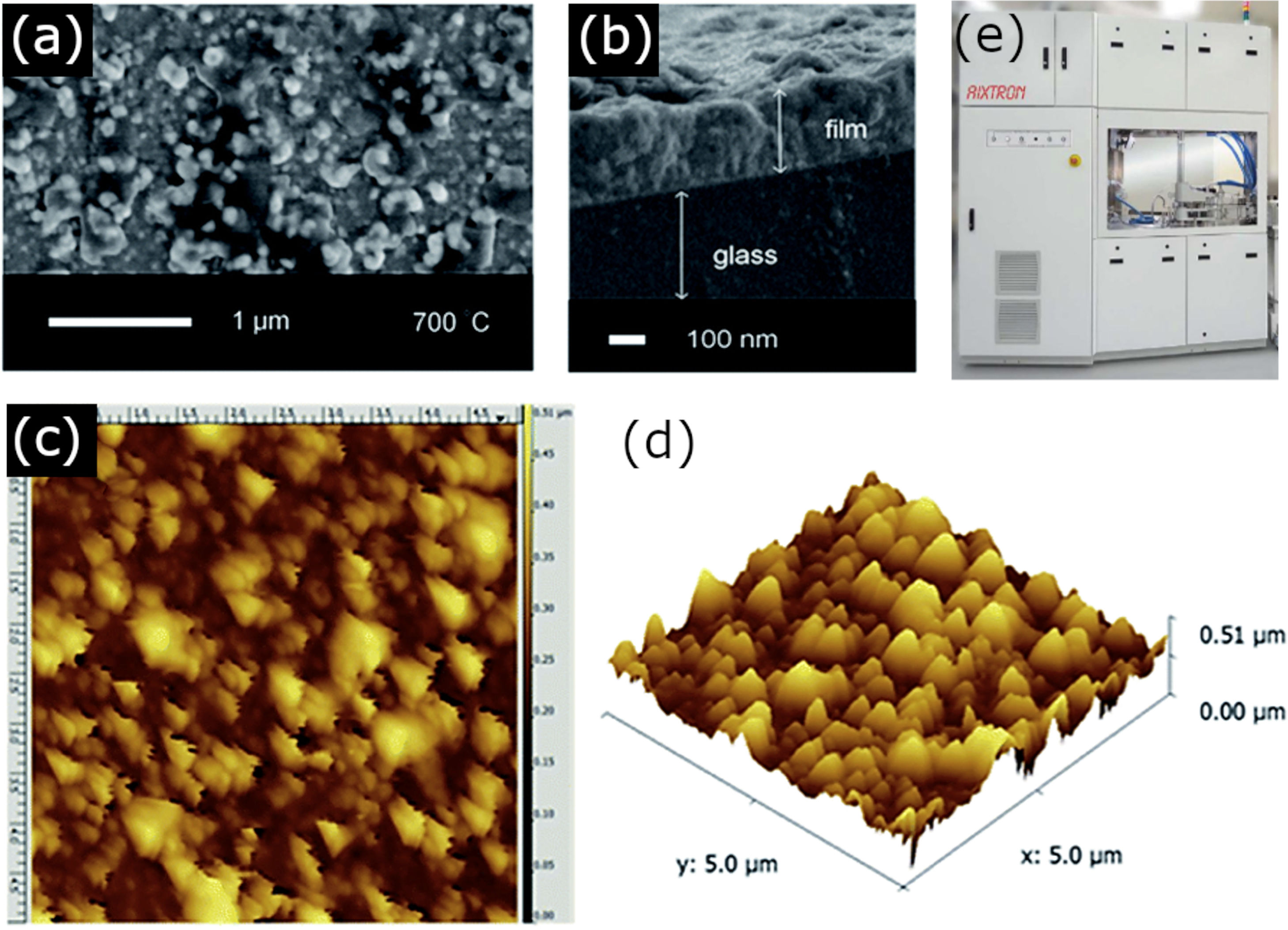
As mentioned, the second block of techniques using a vapor (or plasma) phase medium for the deposition of the films, falls under the CVD methodology and requires a chemical reaction between the vapor/plasma phase precursors on the substrate. Compared to physical methods, the accuracy of CVD techniques might be lower, but they still allow monolayers of deposited material to be obtained and without requiring such high vacuum pressures and expensive equipment. However, this methodology also comes with some drawbacks. The search for the ideal precursor gases or the optimum reaction conditions to give a product with the appropriate composition and stoichiometry can be highly arduous. In the specific case of BiFeO3, problems also arise from the ease of bismuth to volatilize, so the selection of the bismuth precursor becomes an essential parameter. For example, Moniz et al. [67]. used the following non-volatile complex precursor: [CpFe(CO)2·BiCl2], which resulted from the chemical reaction between [CpFe(CO)2]2 and BiCl3, to deposit BiFeO3 thin films with an efficient room-temperature ferromagnetic and ferroelectric order. The authors also studied the effect of different calcination temperatures after the CVD process, observing the unavoidable formation of secondary phases in all the samples treated below 700°C (Fig. 4).
CVD for the obtaining of BiFeO3 thin films. (a) A top-down SEM micrograph, (b) side-on SEM micrograph, (c) a 5μm field size AFM image and (d) the corresponding 3D AFM image of the BiFeO3 film obtained after annealing at 700°C. Reproduced with permission. [67] Copyright 2014, Royal Society of Chemistry. (e) CVD equipment. Reproduced with permission. [91] Copyright 2020, Hampstead Psychological Associates.
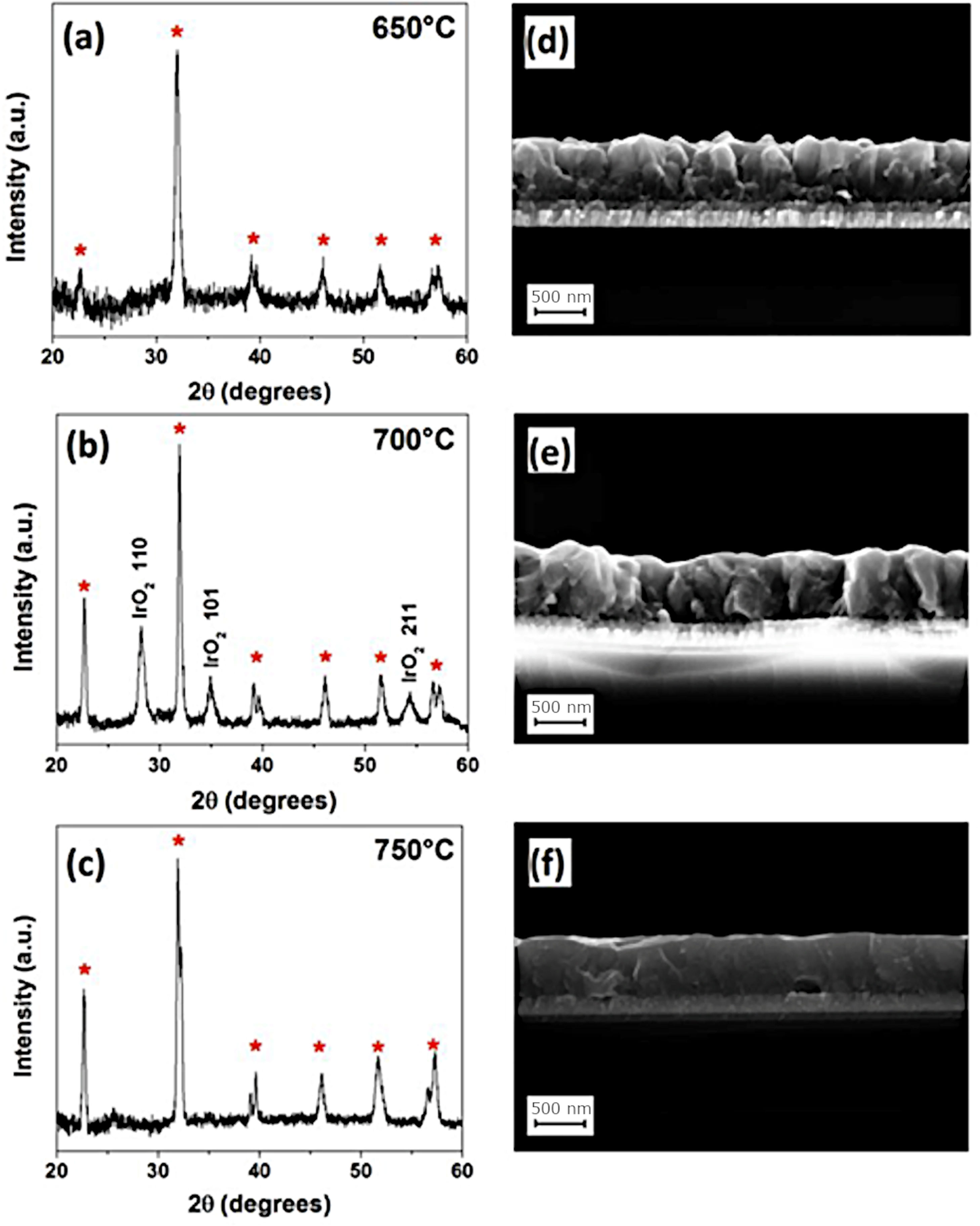
Other authors have tested the possibility of using organometallic reagents as precursors that will react and condense on the surface of the substrate in a process which is known as MOCVD, Metalorganic Chemical Vapor Deposition. This approach allows for greater control of film thickness and facilitates homogeneous doping, and so it has been well received by different groups working on the processing of BiFeO3 thin films. Deepak et al. [93], for example used Fe(thd)3 as an iron precursor to control the Bi-volatilization and therefore the stoichiometry of the material; their films revealed a consistent ferroelectricity (PFM confirmed). Thery and co-workers [95], instead used Fe(tmhd)3 as the iron source and further tested the efficacy of two different bismuth complexes, Bi(tmhd)3 and Bi(mmp)3 as Bi precursors. Initially, the XRD and TEM characterization of the deposited films pointed to the absence of possible parasitic phases, however, a more detailed analysis by XPS did reveal the presence of iron-rich phases which, together with the presence of an observed Fe2+/Fe3+ balance, may be responsible for the good magnetic response of the obtained films as compared to bulk samples; nevertheless, the authors suggest that the use of a single precursor containing both bismuth and iron cations would be the smartest option for a better control of the stoichiometry. Micard et al. [96], on the other hand, have just published a paper showing that pure BiFeO3 films deposited on IrO2/Si substrates can be produced by a MOCVD methodology using Bi(phenyl)3 and Fe(tmhd)3 as metal precursors, once again showing that an appropriate selection of reagents and precursors and, in general, any modification in the processing conditions applied, can be a determinant factor (Fig. 5).
MOCVD for the obtaining of BiFeO3 thin films. XRD diffraction patterns and FESEM cross section micrographs of BifeO3 thin films deposited at (a, d) 650°C, (b, e) 700°C, and (c, f) 750°C. Reproduced with permission. [96] Copyright 2020, MDPI.
The main results obtained with each of these processing methods have been recopilated in Table 1, and in summary, while it is clear that plasma or vapor phase deposition techniques constitute an interesting group of processing strategies to produce BiFeO3 films with a functional response that can be exploited, the contradictions that have been described also reveal certain disadvantages and reproducibility problems. On the one hand, although most of these techniques guarantee a high crystallinity rate that could (a priori) provide a solid multiferroic performance, the control of stoichiometry still remains a serious drawback that is not easy to solve on a practical level; specifically, the high volatility of bismuth can become critical when using some of these procedures, so the difficulty of reducing or eliminating the formation of (unwanted) secondary phases is still very much present in many of the investigations envisaged. On the other hand, all these techniques imply a high energy consumption in terms of temperature and/or vacuum (ultra-high vacuum occasionally), which in turn translates into a high economic cost of the equipment involved and a high degree of sophistication in the production line. On this basis, and in the interest of greater simplicity, environmental benevolence and economic efficiency, the use of processing alternatives with which to obtain BiFeO3 thin films in a more sustainable way is a growing trend in recent years [97,98]. Moreover, by reducing the energy involved in the manufacturing process, the spectrum of accessible materials is significantly broadened, and so the use of volatile substances and metastable compounds such as BiFeO3 itself, is no longer an obstacle. Needless to say, the increase in sustainability also has its trade-offs, but even so, the following section describes some of the most successful techniques in this respect.
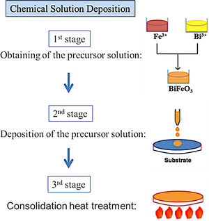
BiFeO3 thin film processing through deposition methods based on liquid phase transportation: chemical solution depositionSolution deposition methods, often labelled under the acronym CSD which stands for “Chemical Solution Deposition”, are at the core of the novel processing approaches currently being developed to obtain multiferroic BiFeO3 thin films in a simple and sustainable way. In these methods, the medium for transporting the precursors to the substrate is a liquid. In a typical procedure, the precursors are dissolved in a first stage of the applied routine and the obtained solution is subsequently deposited on the substrate in a second stage. Finally, a heat treatment at a mild-to-low temperature results in a homogeneous, dense, consolidated and continuous thin film throughout the entire substrate. A schematic plot of the general process is depicted in Fig. 6.
In addition to the implicit low energy consumption, the CSD methodology can also provide high homogeneity, as well as high morphological control on the deposited film by varying the composition, the viscosity of the solution, its pH, or its concentration [99].
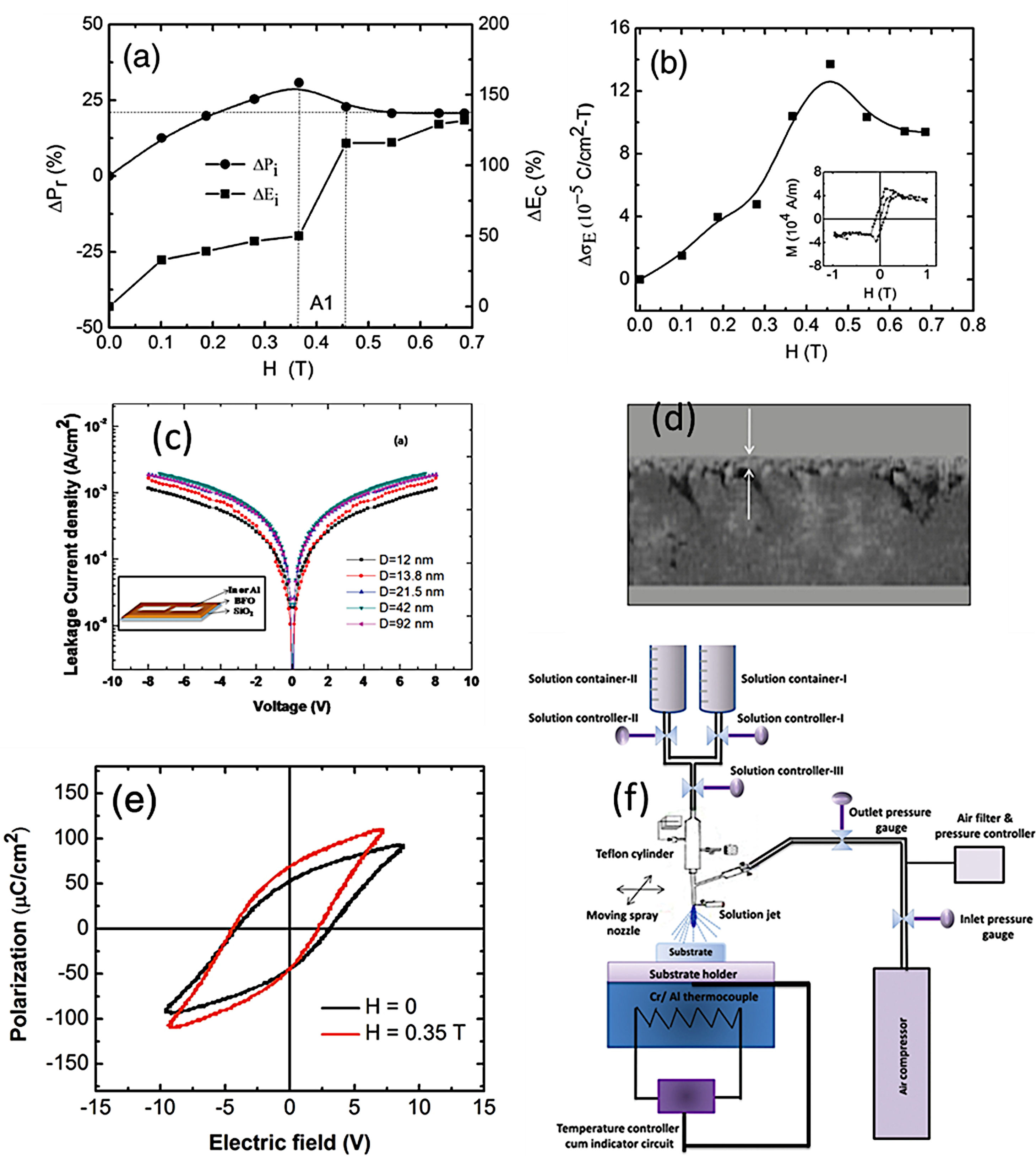
As mentioned above, the CSD methodology comprises three main stages (heat treatment included) which are experimentally accomplished by applying different techniques. For the first step of dissolving the precursors, soft chemistry routines such as the sol–gel process, different chelation processes, or the so-called metall-organic decomposition process (MOD) are often practiced. For the second stage of depositing the precursor solution on the substrate, techniques such as spray-coating (deposition from an aerosol), dip-coating (coating by immersion), or spin-coating (deposition by centrifugation) can be listed [100]. With varying degrees of success, different combinations of these techniques and routines have been attempted, but so far the most common and reliable is perhaps that which uses the sol–gel process to dissolve the (precursor) cations of interest, followed by a dip-coating or a spin-coating procedure for deposition. However, it must be mindful that there are also some published articles in the specialized literature in which BiFeO3 films have been obtained with promising optical, electrical, magnetic and even magnetoelectric properties by spray-coating (Fig. 7) subsequently after the sol–gel process [101,102], but certainly, the number of these articles is considerably fewer.
Sol–Gel+Spray-Coating for the obtaining of BiFeO3 thin films. (a) Magnetic field dependence of remanent polarization and coercive field. (b) The variation of magnetoelectric coupling coefficient with magnetic field (inset: M–H loop) for BiFeO3 films. Reproduced with permission. [102] Copyright 2013, Elsevier. (c) Typical leakage current data of the BiFeO3 films varying from 1.0×10⁻³ to 1.8×10⁻³A/cm2 at 8V with increase grain size in the films. Inset: schematic drawing of device structure. Reproduced with permission. [101] Copyright 2011, AIP Publishing. (d) Cross-sectional micrograph of the BiFeO3 film. (e) Ferroelectric hysteresis loops of BiFeO3 films with and without applied magnetic field with particle size of ∼63nm. Reproduced with permission. [102] Copyright 2013, Elsevier. (f) Spray-pyrolysis experimental set-up. Reproduced with permission. [101] Copyright 2011, AIP Publishing.
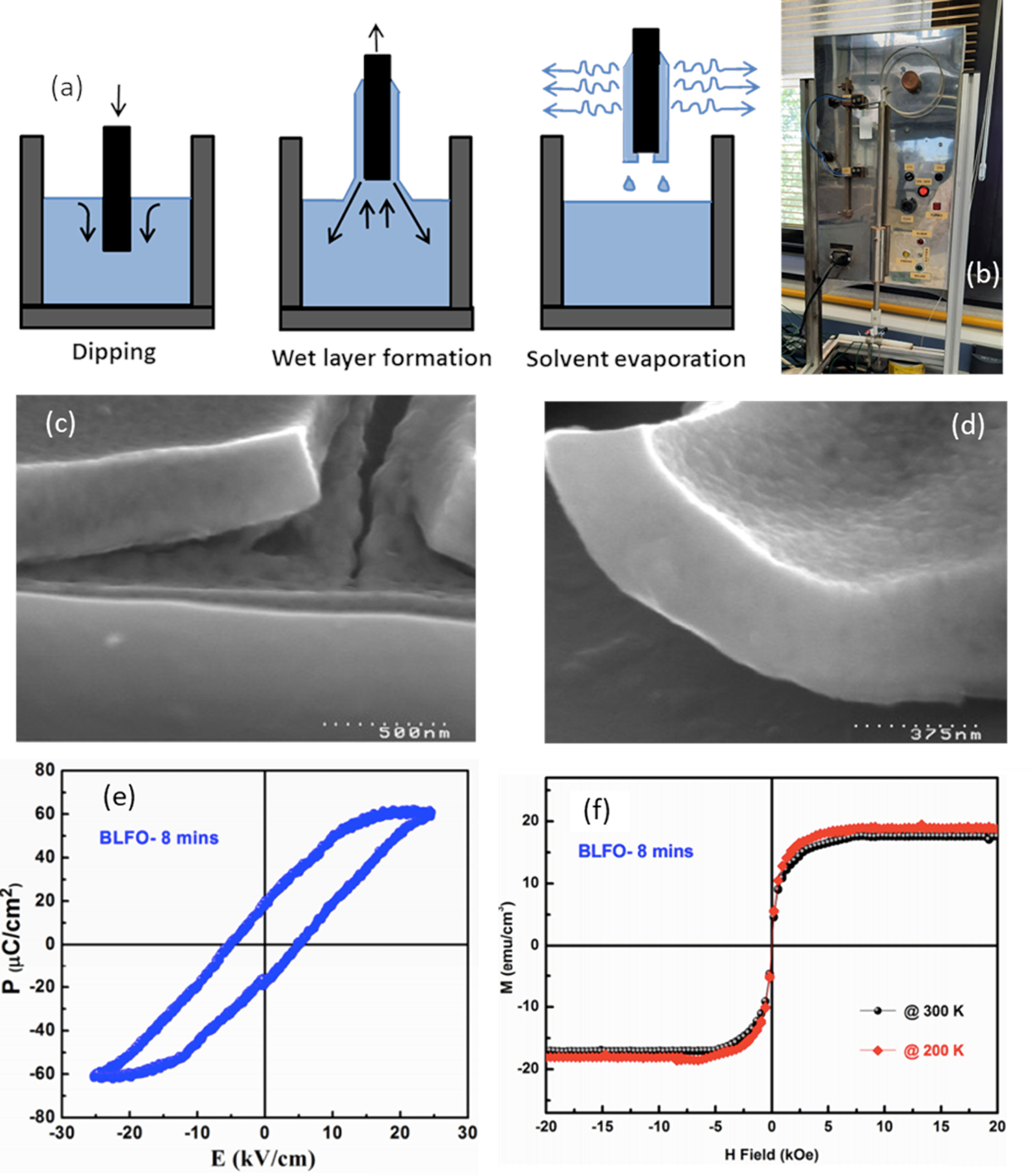
For the first stage, two types of sol–gel approaches have been extensively tested, one starting from colloidal dispersions and the other one from alkoxides [103,104]. In the first case, colloidal particles, isolated or mixed with alkali or alkaline earth ions, are dispersed in a liquid medium. The destabilization of the sol through the addition of electrolytes causes the subsequent gelation. The gel is dried and sintered, normally at temperatures close to 1000°C. These high temperatures are somewhat contrary to the goal of sustainability and, in fact, even being the easiest sol–gel type process to operate, it is not used as often [105]. In the second case the sol is produced by hydrolysis and polycondensation reactions of metallorganic derivatives in alcoholic solutions; it involves the use of alcohols to dissolve the metal precursors and thus form metal alkoxides, which exhibit high reactivity in the presence of water. The most commonly used alcohols are methanol, ethanol, 2-methoxyethanol, and 1,3-propanediol [106,107]. The obtained alkoxide is then hydrolyzed by reacting with a water molecule. Once the hydrolysis reaction has started, two partially hydrolyzed molecules can join by means of a condensation reaction, producing chains of MOM nature, releasing a molecule of water or alcohol. Through hydrolysis and condensation reactions it is possible to create more or less branched networks or structures (the gel) [103–105,108,109]. Actually, 2-metoxyethanol is widely used for the OH group exchange reaction in which metal alkoxide is formed due to its bidentate nature, leading to the formation of an alcoxide less prone to hydrolisis, allowing an easy gel formation rather than precipitation [110]. Additionally, acids, such us acetic acid, or bases are often used as catalysts species of the involved reactions and/or as chelating agents [111], since they prevent the excessive tendency of alkoxides to react thus blocking uncontrolled reactions [100]. In the obtaining of BiFeO3 thin films, it is frequently to use bismuth nitrate (in excess to compensate possible Bi2O3 volatilization) and iron nitrate as metal precursors for the preparation of solutions in this first sol–gel stage. Additionally, on many occasions, ethanolamine is added to adjust the viscosity, which is particularly essential when it is subsequently deposited by spin-coating. The final solutions are typically prepared from 0.1M to 0.3M concentrations [54,112], being 0.2M the most common [34,111,113]. Once the solution is formed is next deposited by dip-coating or spin-coating (as indicated other techniques are less common). In both cases the deposition is carried out on oriented substrates in which an epitaxial growth of the BiFeO3 grains has been observed; this yields satisfactory results in terms of obtaining BiFeO3 thin films in absence of secondary phases and with an interesting functional response. Specifically, in the dip-coating routine, the substrate is immersed in the precursor solution for an optimized time so that when it is extracted, a film of the liquid is dragged and remains adhered to the substrate, thus covering it completely. The subsequent drying and crystallization treatments are then carried out. The formation of the film on the substrate surface is due to the mechanical fluid balance between the entrained film and the receding liquid (Fig. 8a and b). This balance is governed by various forces; viscous resistance and gravitational forces play the most important role, but forces such as surface tension, inertial force or pressure also play a relevant role [114]. A competition between these forces in the region of deposition of the film eventually governs its thickness [100]. Bearing this in mind, Fruth and co-workers [115] used this sol–gel plus dip-coating processing strategy and obtained BiFeO3 films with different thickness (Fig. 8c and d), density and optical constants after subtly playing with the processing parameters; they also tested the possibilities of different chelating agents such as citric acid and polyvinyl alcohol. Later, Hu et al. [116] achieved the preparation of non-doped BiFeO3 thin films and BiFeO3 thin films doped with 30% of La3+ by sol–gel+dip-coating on ITO substrates. These authors observed a rhombohedral perovskite-like structure in the undoped sample, while a distorted structure was produced in the doped one. In addition, they confirmed an improvement in both the magnetic and ferroelectric response with the doping of the material (Fig. 8e and f). In a more recent publication, B. G. Park [117], however, suggests that this sol–gel+dip-coating methodology is also not free from the usual problems surrounding BiFeO3 production, as the thin films obtained also show the presence of a bismuth-rich secondary phase.
Sol–Gel+Dip-Coating for the obtaining of BiFeO3 thin films. (a) Scheme for the dip-coating process. Reproduced with permission. [105] Copyright 2020, Université de Montpellier. (b) Dip-Coating equipment. (c) and (d) SEM micrographs of the BiFeO3 thin films after two annealing treatments at 500°C/1h in which the chelating agent used was citric acid and polyvinyl alcohol respectively. Reproduced with permission. [115] Copyright 2007, Elsevier. (e) and (f) Ferroelectric hysteresis loops and M–H loops at different temperatures for a BiFeO3 thin film doped with 30% of La3+. Reproduced with permission. [116] Copyright 2016, Trans Tech Publications Ltd.
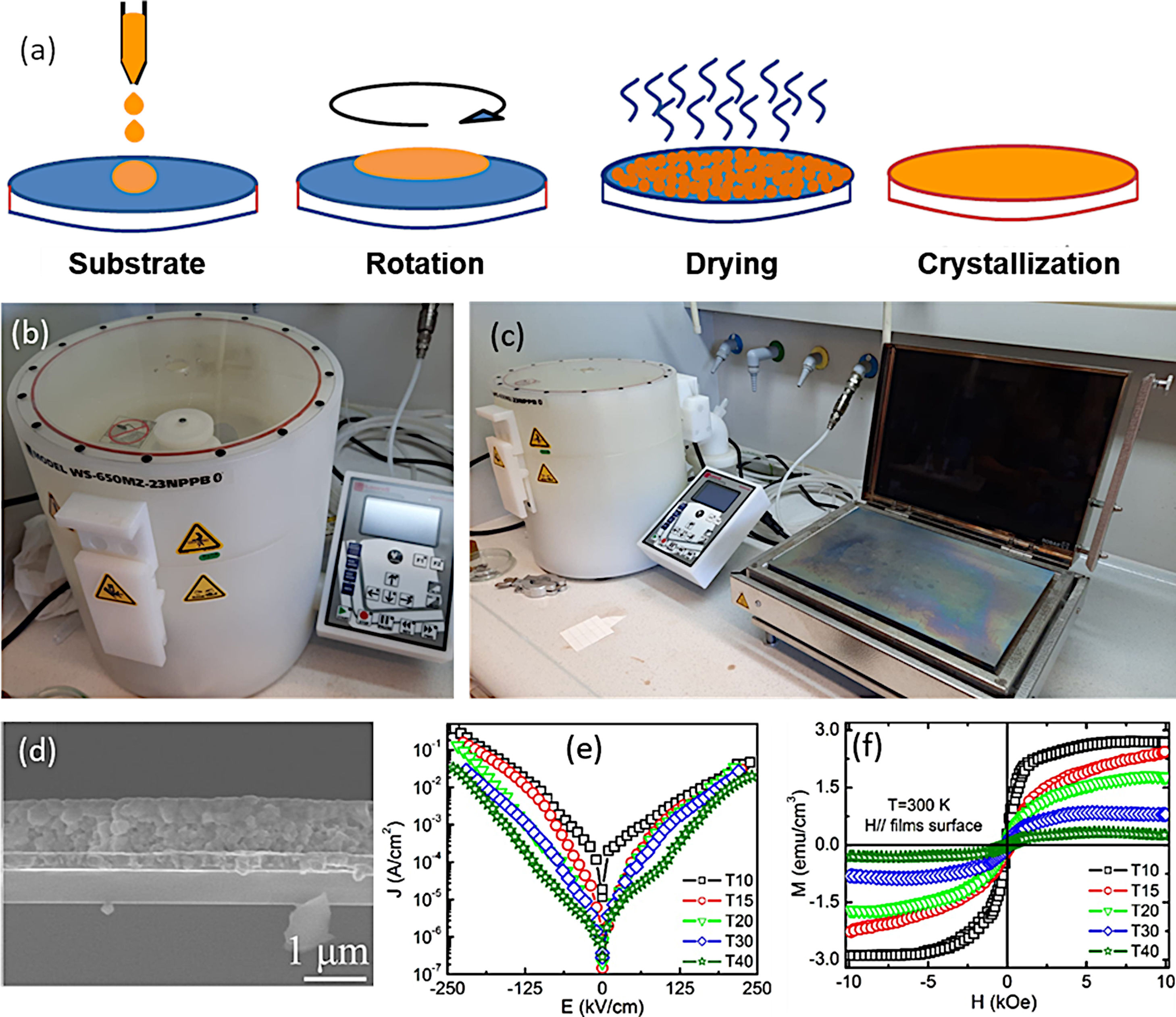
Alternatively to the dip-coating procedure, the spin-coating approach is also widely used. The process mainly involves the deposition of the precursor solution onto a substrate which rotates in a horizontal plane at a certain speed and for a certain time. Centrifugal forces generated by the rotation expand the solution throughout the substrate until it is completely covered [118]. The substrate is kept fixed on the rotating disc by applying vacuum, thus, while the disc rotates, the substrate rotates too. During the time in which the substrate remains rotating, the excess liquid runs off the edges in a drainage process and the speed of elimination of the liquid decreases as the thickness of the film increases, due to the increased viscosity [117]. After the rotation, a drying treatment is applied to remove the remaining solvent and reagents, followed by a drying stage and a crystallization treatment to consolidate the deposited film (Fig. 9a–c). One of the main advantages of the spin-coating deposition process would be related with the film thickness, which becomes uniform during the drainage stage. This is due to the fact that the viscosity does not depend on the shear and so it does not vary on the substrate. During drainage, the centrifugal force is higher than the force of gravity, generating a rapid thinning of the layer. The film reaches its final thickness by evaporation after it becomes thin and viscous enough that it does not flow. In this context, many authors claim to achieve a pure BiFeO3 phase with an interesting functional response in the form of a thin film by means of a sol–gel+spin-coating methodology [40,112,113,119–128]. Tang et al. [40,120], for example, published several articles in which they managed to obtain well-consolidated BiFeO3 films (Fig. 9d), further studying how the electrical and magnetic properties vary as a function of thickness [40] (Fig. 9e and f) and grain size [120]. These authors also demonstrated that the concentration of the precursor solution has a direct influence on the thickness of the deposited films (the higher the concentration, the thicker the film), but also on their functional microstructure and the resulting physical properties [54]. In another article, Quan et al. [58], observed a notable increase in the remnant polarization and a significant decrease in dielectric losses when doping BiFeO3 films with 20% Ce3+. They attribute this improvement in electrical properties to a different Fe3+/Fe2+ balance in the doped films. However, the sol–gel+(spin/dip)-coating technology is also not immune to the usual drawbacks of the BiFeO3 synthesis. In particular, the undesirable presence of secondary phases also remains a major challenge, and is currently triggering the design of alternative processing strategies with which the single-phase material could be produced without scarifying the sustainability goal. Such is the case of the aqueous-based methodology described in the following subsection.
Sol–Gel+Spin-Coating for the obtaining of BiFeO3 thin films. (a) Scheme for the spin-coating process. (b) and (c) Spin-Coating equipment including a hot plate in (c) used for the drying stage. (d) Cross-sectional FESEM micrograph of a BiFeO3 film obtained by sol–gel+spin coating, in which the spinning process has been repeated 40 times (830nm thickness). (e) Room temperature leakage current of BiFeO3 thin films with different thickness. (f) M–H hysteresis loops of BiFeO3 films with different thickness at 300K. Reproduced with permission. [40] Copyright 2011, The American Ceramic Society.
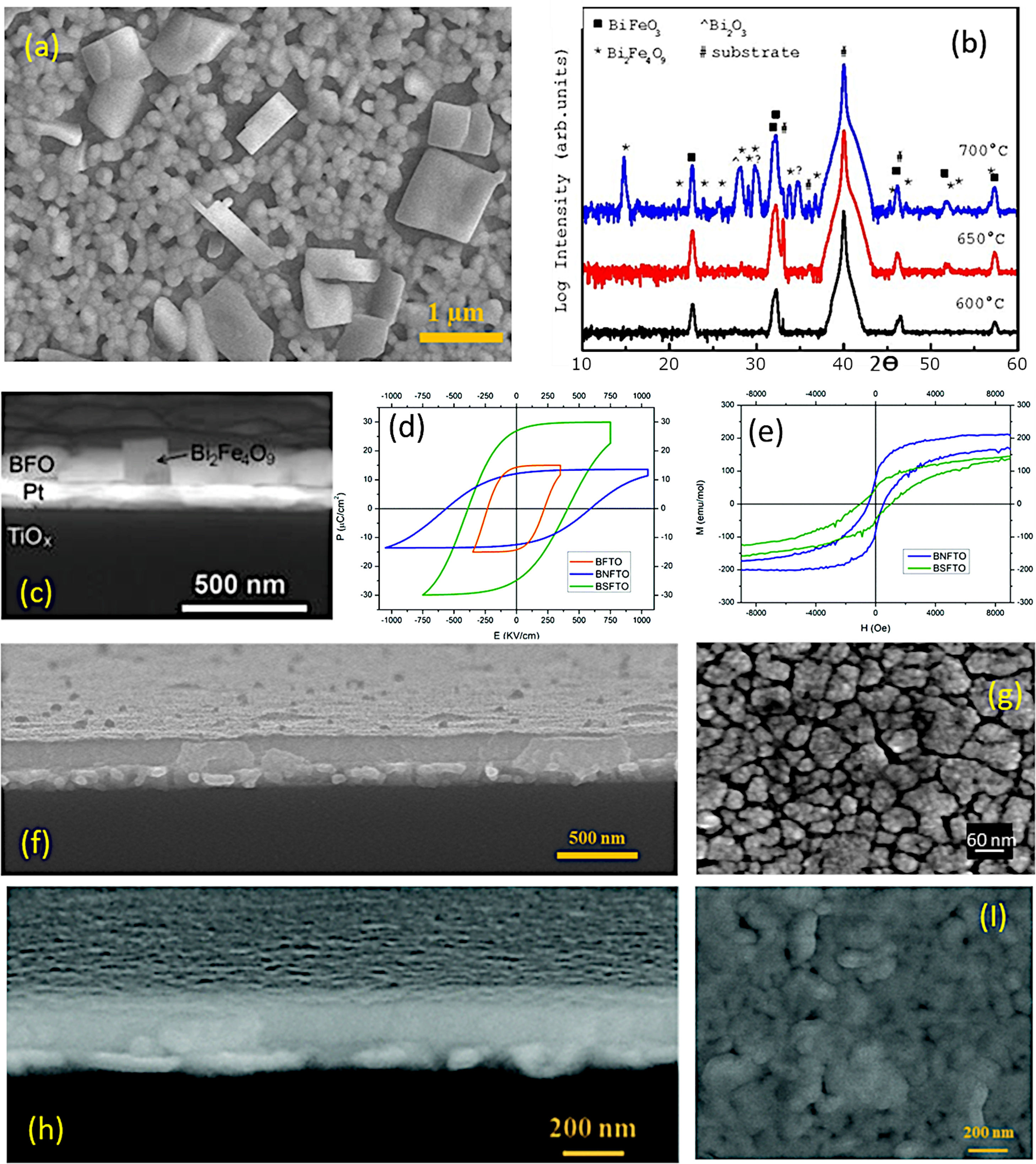
As indicated, a recent alternative to obtain BiFeO3 films in a sustainable fashion is based on applying the sol–gel+spin-coating (or dip-coating) routine described above but introducing a variant which consists on preparing the precursor solution (the “sol”) in aqueous medium. In doing so, the toxic organic solvents used in the conventional sol–gel method to dissolve the metallic precursors (e.g. 2-methoxyethanol), can be avoided, further inciding on the sustainability of the process. The technique is based on using aqueous solutions of the precursors, in which the metal ions of interest are stabilized in complexes with chelating ligands such as peroxides or citrates [129]. These homogeneous precursor solutions are stable under room temperature and pressure for long periods of time, and once they have been formed, they are ready to be deposited on a suitable substrate by spin-coating (or dip-coating [130]) to obtain thin films. After deposition, any residual solvent and any agent added to the starting solution is thermo-oxidatively removed by means of an optimized heat treatment to eventually produce the pure phase of the metal oxide. The methodology provides excellent compositional control (due to the high degree of homogeneity), is cost-effective, and allows easy deposition of films with a thickness rate from several hundred nanometers to a few nanometers [131]. Accordingly, a number of recent articles can be found where BiFeO3 thin films with good control over the parasitic phases can be produced by dissolving the metallic precursors in an aqueous medium [51,113,130,132,133]. In a typical procedure, the precursors of the metals of interest (bismuth, iron and dopants, when used) are first dissolved as individual aqueous solutions. As indicated above, this solution stage involves the use of chelating agents to form stable complexes, such as citric acid or derived citrates [134–136], and so the most widely used precursors iron are bismuth citrate (Bi(C6H5O7)3) and iron citrate (Fe(C6H5O7)3); similar compounds are used for any other metals being present in the starting formulation. The individual solutions are next combined into a single BiFeO3-based multi-metal precursor solution (always keeping the Fe:Bi stoichiometry at the required 1:1 ratio), and this is the one which will be then deposited on the substrate by spin-coating, dip-coating or similar procedures. A characteristic feature of this innovative methodology is that the substrate requires a pre-treatment that makes its surface hydrophilic (we are working in aqueous medium), otherwise there is a risk that the deposited solution will accumulate heterogeneously only at certain points of the substrate. There are several options for this purpose. One of them consists on treating the substrates under an ultraviolet lamp that breaks the atmospheric oxygen causing free radicals, which can react with other O2 molecules generating O3 that will be subsequently adhered to the surface of the substrate, making it hydrophilic. Another practice is to introduce the substrate in a mixture of sulfuric acid and hydrogen peroxide in a 4:1 ratio respectively. This allows OH groups to adhere to the surface, making it hydrophilic as well [137,138]. Once the substrate has been properly pre-treated, the deposition of the multi-metal solution can be carried out, followed by the subsequent drying treatment. As in the non-aqueous methology, the pyrolysis phase (drying) must be divided into several steps, although the different solvent entails a different firing scheme. Otherwise morphological heterogeneities and defects such as fissures and cracks could be generated due to sudden evaporation or uncontrolled (simultaneous) decomposition of the different solution reactants [113,139]. This drying is applied each time a new deposition is performed and, in fact, the total number of depositions (layers), i.e. the number of times the whole deposition+drying protocol is repeated (the crystallization treatment is only carried out once, after all the required layers have been deposited and dried), represents itself a crucial parameter when using this aqueous methodology. The number of layers determines the final thickness of the film, but is also affects the stabilization of the BiFeO3 phase. In particular, a low number of layers/depositions can condition the homogeneity of the films (uncoated regions on the substrate), but may also prevent obtaining the single-phase material: when dealing with thicknesses of just a few tens of nanometres and, therefore, with high surface-to-volume ratios, the Bi-vaporisation, the subsequent Bi deficiency and the consequent formation of the iron-rich Bi2Fe4O9 phase are again favoured (Fig. 10a). The situation can be partially amended by increasing the amount of deposited layers, but also assuming that a high number of depositions could lead to the appearance of micro-cracks in the films [40]. This other inconvenience is actually due to the residual stresses created by the mismatch of the thermal expansion coefficients between the deposited layers: after each deposition, a new a drying process is carried out and this means that the first deposited layers indeed accumulate several pyrolysis treatments. Finally, the whole procedure ends with a crystallization treatment which also has its science. For example, it has been observed that annealing temperatures above 600°C favour the presence of secondary phases such as the iron-rich Bi2Fe4O9 mullite [51]; Again, this occurs as a direct consequence of the volatilization of bismuth, which in this case increases with increasing temperature (Fig. 10b and c). Moreover, the interaction with the platinum substrate may further contribute to this effect, since at high temperature bismuth can also diffuse from the film into the substrate, accumulating beneath the Pt-layer of the electrode or even forming a PtBi alloy [140,141]. With all this in mind, our research team has recently succeeded in obtaining a suitably doped, phase-pure BiFeO3 thin film material applying an aqueous solution-gel process plus spin-coating deposition strategy [133]. Our experiments indicated high reliability for the tested methodology, allowing for the production of homogeneous dense films at temperatures as low as 600°C and with a tuneable multiferroic response (Fig. 10d–i). The whole process is conducted in water, no vacuum settings nor sophisticated equipment is required and despite the low temperature processing conditions, an effective microstructural control is achieved at the nanoscale, which is attributed to effective pinning of the dopants inside the BiFeO3 perovskite structure of since the very beginning of the ferrite formation in the film. This avoids extensive diffusion or segregation of the dopants to the grain boundaries [17,142] as well as to the film interfaces [143], and further facilitates the stabilization of the parent perovskite compound against the formation of unwanted secondary phases.
Aqueous Solution-Gel+Spin-Coating for the obtaining of BiFeO3 thin films. (a) FESEM micrograph of a BiFeO3 thin film surface obtained through three deposition steps. The large squared-shape grains can be ascribed to a Bi2Fe4O9 mullita-type phase. (b) XRD patterns after annealing at 600, 650, or 700°C during 1h. (c) Cross-Sectional FESEM micrograph of a BiFeO3 film annealed at 700°C. Reproduced with permission. [51] Copyright 2015, Springer. (d) P–E hysteresis loops at 140K of three BiFeO3 films doped with titanium (orange curve), neodymium (blue curve) and samarium (green curve). (e) M–H hysteresis loops at 4K of two BiFeO3 films doped with neodymium (blue curve) and samarium (green curve). Reproduced with permission. [133] Copyright 2020, The Royal Society of Chemistry. (f) Cross-sectional FESEM micrograph of a 5-layered BiFeO3 thin film annealed at 600°C during 1h. (g) Surface FESEM micrograph of a 5-layered based BiFeO3 film annealed at 600°C during 1h. Reproduced with permission. [113] Copyright 2018, Elsevier. (h) Cross-sectional FESEM micrograph of an 8-layered based BiFeO3 thin film annealed at 600°C during 1h. (I) Surface FESEM micrograph of an 8-layered based BiFeO3 film annealed at 600°C during 1h. Reproduced with permission. [133] Copyright 2020, The Royal Society of Chemistry.
The main results obtained with each of these processing methods that involve a liquid medium for the precursor transportation to the substrate (CSD methods) have been summarized in Table 2. As depicted, all of these techniques (including those which requires a high energy consumption and sophistication) allow the obtaining of BiFeO3 films with a functional response that can be exploited. However, there are still contradictions that have been described throughout the specialized literature, which highlights the controversy that also exists in the use of this methodology. Nevertheless, all of them present a common aspect: it is clear that the CSD techniques reduce the energy consumption, which inevitably occurs in techniques that use a vapor or plasma phase, and they imply an evident simplicity in their equipment. Moreover, the alternative of the CSD methods which uses an aqueous medium increases even more the sustainability of this techniques for the simple fact of avoiding the use of the organic solvents typically used in a conventional sol gel method, keeping therefore an eye on environmental aspects. As has been demonstrated, the aqueous solution-gel+spin-coating method allows the obtaining of a homogeneous and uniform film at relatively low temperature avoiding the use of the mentioned organic solvents and without the need to set vacuum pressures [130,144], thus emphasizing the simplicity and sustainability of the process.
Summary containing the main results obtained in the synthesis of BiFeO3 thin films by using Chemical Solution Deposition techniques.
| Low energy consumption techniques (based on a liquid phase transportation): CSD | |||||
|---|---|---|---|---|---|
| Processing method | Film composition | Substrate | Film thickness | Functional properties | Ref. |
| Conventional sol–gel method | |||||
| +Spry coating | BiFeO3 | Ultra cleaned glass substrate | Measured in the range of 1.8–2.2μm | Large band gap for small grain size films (12nm): e.g. ∼3.2eV. Low leakage current in the smaller grain size films. | [101] |
| BiFeO3 | Glass substrate | 1.8μm | Ps and Ec values are doubled when the particle size varied from 12 to 42nm. Strong coupling between the magnetic and the ferroelectric orders at room temperature decreasing with particle size. | [102] | |
| +Dip coating | BiFeO3 | Glass, quartz and indium doped tin oxide (ITO) substrate. | 2μm | Multiferroic response observed. Both hysteresis curves failed to attain saturation. Films ∼90% transparency (e.g. ∼2.88–3.03eV) | [45] |
| BiFeO3 and Bi0.7La0.3FeO3 | Glass/ITO substrate | – | Ms increases from 4.59emu/cm3 to 17.13emu/cm3 with 30% Bi3+ substituted by La3+. 2Pr and 2Ec vary from 31.8μC/cm2 and 29.5kV/cm to 39.2μC/cm2 and 10.5kV/cm. Photovoltaic effect in Bi0.7La0.3FeO3 thin film. | [116] | |
| BiFeO3 | Polycarbonate surface | – | Films absorbing UV and visible light up to 600nm. E.g. ∼2.3eV, suggesting photocatalytic activity in visible region. | [117] | |
| +Spin coating | BiFeO3 | Pt/Ti/SiO2/Si (100) substrate | 210–830nm | Effect of increasing thickness: Dielectric constant enhanced, leakage current reduced, magnetization and magnetodielectric decreased. Optimized thickness: 400–600nm. | [40] |
| BiFeO3 | n-type Si (100) substrate | 189–474nm | Effect of decreasing individual layer thickness: Magnetization increased (Highest Ms=18.3emu/cm3), dielectric constant decreased, magnetoelectric coupling increased | [54] | |
| Bi1−xCexFeO3 (x=0, 0.05, 0.1, 0.15 and 0.20) | Pt(111)/TiN/Si3N4/Si (100) substrate | – | Pr ∼1.08, 1.43 and 2.04μC/cm2 and Ec ∼120, 112 and 123kV/cm. Leakage current density of the Bi0.8Ce0.2FeO3 capacitor ∼2 orders of magnitude lower than that of the BiFeO3 counterpart. | [58] | |
| BiFeO3 | Pt/Ti/SiO2/Si (100) substrate | ∼560nm | ɛr and tan(δ) increases and decreases within the initial hour. Leakages decrease and then increase with dwell time for ↓T annealing. For ↑T they decrease and then increase and finally decrease again. Ferroelectric Ec is decreased with ↑T annealing. | [120] | |
| BiFeO3 | (111) Pt/Ti/SiO2/Si substrates | 80nm, 100nm and 180nm | Pr=0.36 and 0.88μC/cm2 while Ps=0.69 and 1.87μC/cm2 for 100 and 130nm films. Ms=95emu/cm3 for 130nm films (VSM). Ms=12 and 70emu/cm3 for 100 and 130nm films (SQUID). | [125] | |
| BiFe1−xTixO3 (x=0.05, 0.1, and 0.15) | (111) Pt/Ti/SiO2/Si substrates | ∼190nm | Ti4+-doping increases both Ps and Pr=25.9 and 9.39μC/cm2 (x=0.05) and 32.5 and 16.2μC/cm2 (x=0.1). Leakages lowered one to two orders of magnitude. Ms=21 and 30emu/cm3 (x=0.05 and 0.1). Ms reduced doping with Ti4+. | [126] | |
| BiFeO3BiFe0.07Ti0.03O3BiFe0.07V0.03O3BiFe0.07Cr0.03O3BiFe0.07Mn0.03O3BiFe0.07Co0.03O3BiFe0.07Ni0.03O3BiFe0.07Cu0.03O3BiFe0.07Zn0.03O3 | Silicon (100) substrates | ∼1μm | Ti, V, Mn, Cu and Zn-doping: small increase in Ms. A higher increase with Cr, Co and Ni doping. The highest value of Ms (8.5emu/cm−3) and Hc (173 Oe) occurs in the Cr-doped samples, but negative effect on the electrical properties. High leakages. | [127] | |
| BiFeO3 | Pt/Ti/SiO2/Si (100) substrate and Pt/sapphire (0001) structures | 10–20nm | At 80K, Pr and Ec ∼100μC/cm2 and 0.4MV/cm at 2MV/cm electric applied field. Polarization ∼10% smaller in the film on Si. | [112] | |
| BiFeO3 | Pt/Ti/SiO2/Si(100) | 400nm | Leakage current ∼10−8 A/cm2 at room temperature. Pr ∼90μC/cm2 at 80K and the piezoelectric coefficient d33 ∼50pm/V. | [128] | |
| Aqueous solution-gel method | |||||
| +Dip coating | BiFeO3 | Silica-Soda-Lime glass substrate | 180nm and ∼360nm | Optical properties: Refractive index n up to 1.6 and extinction coefficient k up to 0.12 for λ=0.55μm | [115] |
| BiFeO3 | Stainless steel substrate | A thin sublayer∼100nm and a thicker one <1μm. | – | [130] | |
| +Spin coating | BiFeO3BiFe1−xTixO3, where x=0.05, 0.1, 0.15 or 0.20 | Pt(80nm)/TiOx(30nm)/SiO2/Si substrate | 1-, 3-, 6- and 8-layers. No thickness value reported. | 3-Layered BiFeO3 films BiFeO3 films annealed at 700°C exhibit lower magnetization values. Ti4+-doping reduces Ms further in comparison to non doped films annealed at 700C. | [51] |
| Bi0.88Sm0.12FeO3 and a compositeBi0.88Sm0.12FeO3/Bi3.2Sm0.8Ti3O12 | Si/SiO2 (100) substrate | Single phase∼90nm and composite∼100nm | – | [113] | |
| Bi0.88Sm0.12FeO3Bi0.85Nd0.15FeO3BiFe0.95Ti0.05FeO3.025Bi0.88Sm0.12Fe0.95Ti0.05O3.025Bi0.85Nd0.15Fe0.95Ti0.05O3.025 | Pt(111)Ti/SiO2/Si substrate | 250nm | Ti4+-dpoing: Pr+=15μC/cm2, Mr+=–Sm3++Ti4+-doping: Pr+=27μC/cm2, Mr+=47emu/molNd3++Ti4+-doping Pr+=12μC/cm2,Mr+=77emu/mol | [133] | |
BiFeO3 thin films can be satisfactorily obtained in terms of thickness homogeneity and uniformity along the whole substrate through any of the techniques described: those based on a gas or plasma phase for the precursors transportation to the substrate, including those which may also involve a chemical reaction between precursors, or those based on a liquid precursor solution for the mentioned transportation. However, there is still a strong controversy regarding the technique that provides better results in terms of the absence of secondary phases and an effective functional response. Moreover, there are many parameters that can significantly influence in the searched result and must be taken into account, such as those typically involved in techniques based on rotational and centrifugal forces spreading the precursor solution: the rotation speed, rotation time, solution concentration, solution viscosity, and needless to mention the chosen substrate as well as the corresponding drying and crystallization temperatures. Nevertheless, it seems clear that there is an important difference in the energy consumed by each technique (in terms of temperature and pressure), being the aqueous solution-gel+spin-coating methodology the one involving a higher sustainability from an energetic, ecologic and economical point of view. Beyond the used technique, current and future research in the obtaining of BiFeO3 thin films still at the forefront in the search of functional advanced materials and endeavours its conversion into a technology of practical application. Some of the future research perspectives will focus on advancing with the study of the mechanisms that stabilize the perovskite phase against the secondary phases which typically coexist, something that is already quite advanced in bulk, but in thin films imply tackling new challenges and new frontiers basically due to the nano dimensions of the final material (new phenomena and behaviours occur at the nano scale). On the other hand, parameters of the processing conditions will be further addressed in order to integrate BiFeO3 into flexible electronics, a field that is currently particularly prominent. Likewise, there is a lot of work to be done in the development and optimization of new dopant formulations and/or new compositions (e.g. composite systems), with which to achieve that the usual restrictions derived from the simultaneous coexistence of ferroelectricity and ferromagnetism (and which are even more noticeable in laminar geometry) cease to be a limiting factor and allow, not only a better multiferroic response, but also an effective magnetoelectric coupling that could be applied in commercial devices, which is not yet feasible. It seems clear in any case that the research for BiFeO3 thin films with increasing performance will continue to be a common practice in the coming years, so choosing the most appropriate method will continue to be a critical issue that will also require extensive knowledge.
This work was conducted within the FPI program (Ref: BES-2014-067779). It was supported by the Spanish Ministry of Economy and Competitiveness (MINECO) through MAT2016-80182-R and MAT2013-40722-R projects. D.G.C. also acknowledges the Fundación General CSIC (ComFuturo Program) for the financial support.




![Sputtering for the obtaining of BiFeO3-base thin films. (a) Schematic representation of the mechanism that takes place during the formation of an oxide thin film by sputtering. (b) Bi0.75Ba0.25Fe0.975Ni0.025O3 thin film micrograph obtained by Scanning Electron Microscopy. Reproduced with permission. [75] Copyright 2016, Springer. (c) Ferroelectric hysteresis loop for a BiFeO3 thin film. Reproduced with permission. [85] Copyright 2020, Elsevier. (d) M–H curves for the Bi0.75Ba0.25Fe0.975Ni0.025O3 thin film. Reproduced with permission. [75] Copyright 2016, Springer. (e) BiFeO3 thin film with a profile obtained by EDS for bismuth, iron and the silica of the substrate. Reproduced with permission. [85] Copyright 2020, Elsevier. (f) Thickness decrease for a BiFeO3 thin film with the increase of O2 partial pressure. Reproduced with permission. [75] Copyright 2016, Springer. Sputtering for the obtaining of BiFeO3-base thin films. (a) Schematic representation of the mechanism that takes place during the formation of an oxide thin film by sputtering. (b) Bi0.75Ba0.25Fe0.975Ni0.025O3 thin film micrograph obtained by Scanning Electron Microscopy. Reproduced with permission. [75] Copyright 2016, Springer. (c) Ferroelectric hysteresis loop for a BiFeO3 thin film. Reproduced with permission. [85] Copyright 2020, Elsevier. (d) M–H curves for the Bi0.75Ba0.25Fe0.975Ni0.025O3 thin film. Reproduced with permission. [75] Copyright 2016, Springer. (e) BiFeO3 thin film with a profile obtained by EDS for bismuth, iron and the silica of the substrate. Reproduced with permission. [85] Copyright 2020, Elsevier. (f) Thickness decrease for a BiFeO3 thin film with the increase of O2 partial pressure. Reproduced with permission. [75] Copyright 2016, Springer.](https://static.elsevier.es/multimedia/03663175/0000006100000006/v2_202212200715/S0366317521000728/v2_202212200715/en/main.assets/thumbnail/gr1.jpeg?xkr=ue/ImdikoIMrsJoerZ+w96p5LBcBpyJTqfwgorxm+Ow=)
![PLD for the obtaining of BiFeO3 thin films. (a, b) PLD equipment. Reproduced with permission. [91] Copyright 2020, Hampstead Psychological Associates. (c) Transmission Electron Microscopy micrograph for a BiFeO3 thin film obtained with 2–3nm of thickness on a (110)-NdGaO3 orthorrombic-perovskite oriented substrate by PLD. Reproduced with permission. [80] Copyright 2018, Elsevier. PLD for the obtaining of BiFeO3 thin films. (a, b) PLD equipment. Reproduced with permission. [91] Copyright 2020, Hampstead Psychological Associates. (c) Transmission Electron Microscopy micrograph for a BiFeO3 thin film obtained with 2–3nm of thickness on a (110)-NdGaO3 orthorrombic-perovskite oriented substrate by PLD. Reproduced with permission. [80] Copyright 2018, Elsevier.](https://static.elsevier.es/multimedia/03663175/0000006100000006/v2_202212200715/S0366317521000728/v2_202212200715/en/main.assets/thumbnail/gr2.jpeg?xkr=ue/ImdikoIMrsJoerZ+w96p5LBcBpyJTqfwgorxm+Ow=)
![MBE for the obtaining of BiFeO3 thin films. (a) RHEED image taken during deposition, which is showing a 2-D growth front with a 6-fold surface reconstruction after the growth and anneal of 10 unit cells. (b) High resolution STEM image showing the interface between BFO and the STO substrate. (c) SADP showing BFO grows in a distorted rhombohedral crystal structure. (d) Room temperature magnetic hysteresis curves for a 40nm BiFeO3 film up to 30 KOe. (e) Ms as a function of this film thickness. Reproduced with permission. [82] Copyright 2013, AIP Publishing. (f) MBE equipment for the obtaining of thin films. Reproduced with permission. [94] Copyright 2020, Elsevier. (g) Bright-field TEM micrograph of a 35nm thick 0001-oriented BiFeO3 film. (h) Selected-area electron diffraction from region covering this film and the substrate. Reflections from the SrTiO3 substrate are indexed. (i) HRTEM micrograph of the film/substrate interface. Reproduced with permission. [81] Copyright 2007, AIP Publishing. MBE for the obtaining of BiFeO3 thin films. (a) RHEED image taken during deposition, which is showing a 2-D growth front with a 6-fold surface reconstruction after the growth and anneal of 10 unit cells. (b) High resolution STEM image showing the interface between BFO and the STO substrate. (c) SADP showing BFO grows in a distorted rhombohedral crystal structure. (d) Room temperature magnetic hysteresis curves for a 40nm BiFeO3 film up to 30 KOe. (e) Ms as a function of this film thickness. Reproduced with permission. [82] Copyright 2013, AIP Publishing. (f) MBE equipment for the obtaining of thin films. Reproduced with permission. [94] Copyright 2020, Elsevier. (g) Bright-field TEM micrograph of a 35nm thick 0001-oriented BiFeO3 film. (h) Selected-area electron diffraction from region covering this film and the substrate. Reflections from the SrTiO3 substrate are indexed. (i) HRTEM micrograph of the film/substrate interface. Reproduced with permission. [81] Copyright 2007, AIP Publishing.](https://static.elsevier.es/multimedia/03663175/0000006100000006/v2_202212200715/S0366317521000728/v2_202212200715/en/main.assets/thumbnail/gr3.jpeg?xkr=ue/ImdikoIMrsJoerZ+w96p5LBcBpyJTqfwgorxm+Ow=)
![CVD for the obtaining of BiFeO3 thin films. (a) A top-down SEM micrograph, (b) side-on SEM micrograph, (c) a 5μm field size AFM image and (d) the corresponding 3D AFM image of the BiFeO3 film obtained after annealing at 700°C. Reproduced with permission. [67] Copyright 2014, Royal Society of Chemistry. (e) CVD equipment. Reproduced with permission. [91] Copyright 2020, Hampstead Psychological Associates. CVD for the obtaining of BiFeO3 thin films. (a) A top-down SEM micrograph, (b) side-on SEM micrograph, (c) a 5μm field size AFM image and (d) the corresponding 3D AFM image of the BiFeO3 film obtained after annealing at 700°C. Reproduced with permission. [67] Copyright 2014, Royal Society of Chemistry. (e) CVD equipment. Reproduced with permission. [91] Copyright 2020, Hampstead Psychological Associates.](https://static.elsevier.es/multimedia/03663175/0000006100000006/v2_202212200715/S0366317521000728/v2_202212200715/en/main.assets/thumbnail/gr4.jpeg?xkr=ue/ImdikoIMrsJoerZ+w96p5LBcBpyJTqfwgorxm+Ow=)
![MOCVD for the obtaining of BiFeO3 thin films. XRD diffraction patterns and FESEM cross section micrographs of BifeO3 thin films deposited at (a, d) 650°C, (b, e) 700°C, and (c, f) 750°C. Reproduced with permission. [96] Copyright 2020, MDPI. MOCVD for the obtaining of BiFeO3 thin films. XRD diffraction patterns and FESEM cross section micrographs of BifeO3 thin films deposited at (a, d) 650°C, (b, e) 700°C, and (c, f) 750°C. Reproduced with permission. [96] Copyright 2020, MDPI.](https://static.elsevier.es/multimedia/03663175/0000006100000006/v2_202212200715/S0366317521000728/v2_202212200715/en/main.assets/thumbnail/gr5.jpeg?xkr=ue/ImdikoIMrsJoerZ+w96p5LBcBpyJTqfwgorxm+Ow=)
![Sol–Gel+Spray-Coating for the obtaining of BiFeO3 thin films. (a) Magnetic field dependence of remanent polarization and coercive field. (b) The variation of magnetoelectric coupling coefficient with magnetic field (inset: M–H loop) for BiFeO3 films. Reproduced with permission. [102] Copyright 2013, Elsevier. (c) Typical leakage current data of the BiFeO3 films varying from 1.0×10⁻³ to 1.8×10⁻³A/cm2 at 8V with increase grain size in the films. Inset: schematic drawing of device structure. Reproduced with permission. [101] Copyright 2011, AIP Publishing. (d) Cross-sectional micrograph of the BiFeO3 film. (e) Ferroelectric hysteresis loops of BiFeO3 films with and without applied magnetic field with particle size of ∼63nm. Reproduced with permission. [102] Copyright 2013, Elsevier. (f) Spray-pyrolysis experimental set-up. Reproduced with permission. [101] Copyright 2011, AIP Publishing. Sol–Gel+Spray-Coating for the obtaining of BiFeO3 thin films. (a) Magnetic field dependence of remanent polarization and coercive field. (b) The variation of magnetoelectric coupling coefficient with magnetic field (inset: M–H loop) for BiFeO3 films. Reproduced with permission. [102] Copyright 2013, Elsevier. (c) Typical leakage current data of the BiFeO3 films varying from 1.0×10⁻³ to 1.8×10⁻³A/cm2 at 8V with increase grain size in the films. Inset: schematic drawing of device structure. Reproduced with permission. [101] Copyright 2011, AIP Publishing. (d) Cross-sectional micrograph of the BiFeO3 film. (e) Ferroelectric hysteresis loops of BiFeO3 films with and without applied magnetic field with particle size of ∼63nm. Reproduced with permission. [102] Copyright 2013, Elsevier. (f) Spray-pyrolysis experimental set-up. Reproduced with permission. [101] Copyright 2011, AIP Publishing.](https://static.elsevier.es/multimedia/03663175/0000006100000006/v2_202212200715/S0366317521000728/v2_202212200715/en/main.assets/thumbnail/gr7.jpeg?xkr=ue/ImdikoIMrsJoerZ+w96p5LBcBpyJTqfwgorxm+Ow=)
![Sol–Gel+Dip-Coating for the obtaining of BiFeO3 thin films. (a) Scheme for the dip-coating process. Reproduced with permission. [105] Copyright 2020, Université de Montpellier. (b) Dip-Coating equipment. (c) and (d) SEM micrographs of the BiFeO3 thin films after two annealing treatments at 500°C/1h in which the chelating agent used was citric acid and polyvinyl alcohol respectively. Reproduced with permission. [115] Copyright 2007, Elsevier. (e) and (f) Ferroelectric hysteresis loops and M–H loops at different temperatures for a BiFeO3 thin film doped with 30% of La3+. Reproduced with permission. [116] Copyright 2016, Trans Tech Publications Ltd. Sol–Gel+Dip-Coating for the obtaining of BiFeO3 thin films. (a) Scheme for the dip-coating process. Reproduced with permission. [105] Copyright 2020, Université de Montpellier. (b) Dip-Coating equipment. (c) and (d) SEM micrographs of the BiFeO3 thin films after two annealing treatments at 500°C/1h in which the chelating agent used was citric acid and polyvinyl alcohol respectively. Reproduced with permission. [115] Copyright 2007, Elsevier. (e) and (f) Ferroelectric hysteresis loops and M–H loops at different temperatures for a BiFeO3 thin film doped with 30% of La3+. Reproduced with permission. [116] Copyright 2016, Trans Tech Publications Ltd.](https://static.elsevier.es/multimedia/03663175/0000006100000006/v2_202212200715/S0366317521000728/v2_202212200715/en/main.assets/thumbnail/gr8.jpeg?xkr=ue/ImdikoIMrsJoerZ+w96p5LBcBpyJTqfwgorxm+Ow=)
![Sol–Gel+Spin-Coating for the obtaining of BiFeO3 thin films. (a) Scheme for the spin-coating process. (b) and (c) Spin-Coating equipment including a hot plate in (c) used for the drying stage. (d) Cross-sectional FESEM micrograph of a BiFeO3 film obtained by sol–gel+spin coating, in which the spinning process has been repeated 40 times (830nm thickness). (e) Room temperature leakage current of BiFeO3 thin films with different thickness. (f) M–H hysteresis loops of BiFeO3 films with different thickness at 300K. Reproduced with permission. [40] Copyright 2011, The American Ceramic Society. Sol–Gel+Spin-Coating for the obtaining of BiFeO3 thin films. (a) Scheme for the spin-coating process. (b) and (c) Spin-Coating equipment including a hot plate in (c) used for the drying stage. (d) Cross-sectional FESEM micrograph of a BiFeO3 film obtained by sol–gel+spin coating, in which the spinning process has been repeated 40 times (830nm thickness). (e) Room temperature leakage current of BiFeO3 thin films with different thickness. (f) M–H hysteresis loops of BiFeO3 films with different thickness at 300K. Reproduced with permission. [40] Copyright 2011, The American Ceramic Society.](https://static.elsevier.es/multimedia/03663175/0000006100000006/v2_202212200715/S0366317521000728/v2_202212200715/en/main.assets/thumbnail/gr9.jpeg?xkr=ue/ImdikoIMrsJoerZ+w96p5LBcBpyJTqfwgorxm+Ow=)
![Aqueous Solution-Gel+Spin-Coating for the obtaining of BiFeO3 thin films. (a) FESEM micrograph of a BiFeO3 thin film surface obtained through three deposition steps. The large squared-shape grains can be ascribed to a Bi2Fe4O9 mullita-type phase. (b) XRD patterns after annealing at 600, 650, or 700°C during 1h. (c) Cross-Sectional FESEM micrograph of a BiFeO3 film annealed at 700°C. Reproduced with permission. [51] Copyright 2015, Springer. (d) P–E hysteresis loops at 140K of three BiFeO3 films doped with titanium (orange curve), neodymium (blue curve) and samarium (green curve). (e) M–H hysteresis loops at 4K of two BiFeO3 films doped with neodymium (blue curve) and samarium (green curve). Reproduced with permission. [133] Copyright 2020, The Royal Society of Chemistry. (f) Cross-sectional FESEM micrograph of a 5-layered BiFeO3 thin film annealed at 600°C during 1h. (g) Surface FESEM micrograph of a 5-layered based BiFeO3 film annealed at 600°C during 1h. Reproduced with permission. [113] Copyright 2018, Elsevier. (h) Cross-sectional FESEM micrograph of an 8-layered based BiFeO3 thin film annealed at 600°C during 1h. (I) Surface FESEM micrograph of an 8-layered based BiFeO3 film annealed at 600°C during 1h. Reproduced with permission. [133] Copyright 2020, The Royal Society of Chemistry. Aqueous Solution-Gel+Spin-Coating for the obtaining of BiFeO3 thin films. (a) FESEM micrograph of a BiFeO3 thin film surface obtained through three deposition steps. The large squared-shape grains can be ascribed to a Bi2Fe4O9 mullita-type phase. (b) XRD patterns after annealing at 600, 650, or 700°C during 1h. (c) Cross-Sectional FESEM micrograph of a BiFeO3 film annealed at 700°C. Reproduced with permission. [51] Copyright 2015, Springer. (d) P–E hysteresis loops at 140K of three BiFeO3 films doped with titanium (orange curve), neodymium (blue curve) and samarium (green curve). (e) M–H hysteresis loops at 4K of two BiFeO3 films doped with neodymium (blue curve) and samarium (green curve). Reproduced with permission. [133] Copyright 2020, The Royal Society of Chemistry. (f) Cross-sectional FESEM micrograph of a 5-layered BiFeO3 thin film annealed at 600°C during 1h. (g) Surface FESEM micrograph of a 5-layered based BiFeO3 film annealed at 600°C during 1h. Reproduced with permission. [113] Copyright 2018, Elsevier. (h) Cross-sectional FESEM micrograph of an 8-layered based BiFeO3 thin film annealed at 600°C during 1h. (I) Surface FESEM micrograph of an 8-layered based BiFeO3 film annealed at 600°C during 1h. Reproduced with permission. [133] Copyright 2020, The Royal Society of Chemistry.](https://static.elsevier.es/multimedia/03663175/0000006100000006/v2_202212200715/S0366317521000728/v2_202212200715/en/main.assets/thumbnail/gr10.jpeg?xkr=ue/ImdikoIMrsJoerZ+w96p5LBcBpyJTqfwgorxm+Ow=)
