A Solution Based Indium-Zinc-Oxide thin-film transistor (TFT) with a field-effect mobility of 0.58cm2/Vs, a threshold voltage of 2.84V by using pulse laser annealing processes. Indium-zinc-oxide (IZO) films with a low process temperature were deposited by sol-gel solution based method and KrF excimer laser annealing (wavelength of 248nm). Solution based indium-zinc-oxide (IZO) films usually needs high temperature about 500°C post annealing in a oven. KrF excimer laser annealing shows advantages of low temperature process, the less process time deceases to only few seconds was used to replace the high temperature process. IZO thin films suffering laser irradiation still keeps the amorphous film quality by transmission electron microscopy (TEM) diffraction pattern analysis. It could be expected this technology to large-area flexible display, in the future.
Amorphous oxide semiconductors (AOSs) have emerged as one of the most important classes of novel thin-film devices. AOS transistors have a great potential for use in upcoming electronic devices, such as thin-film transistor (TFT) backplanes for active matrix liquid crystal displays (AMLCD) or transparent active matrix organic light-emitting diode displays (AMOLED) and solar cell (Mbodji, Dieng, Mbow, Barro, & Sissoko, 2010). Furthermore, compared with conventional amorphous silicon (a-Si) and polycrystalline silicon (poly-Si) TFT, AOS transistors offer higher mobility, better uniformity and transparency to visible light (Nomura et al., 2004; Fortunato et al., 2005; Jeong et al., 2007; Kim et al., 2007). AOS thin films have been prepared by a variety of thin-film deposition techniques such as RF magnetron sputtering (Park, Maeng, Kim, & Park, 2012; Ku et al., 2006; Pi et al., 2013), pulsed laser deposition (Masuda et al., 2003; Ramamoorthy et al., 2006; Ito et al., 2006; Yaglioglu, Yeom, Beresford, & Paine, 2006), and chemical vapor deposition (Kashiwaba, Katahira, Haga, Sekiguchi, & Watanabe, 2000). Although AOS thin films can be deposited at lower temperatures or even room temperatures by vacuum deposition methods (Jeong, Bae, & Kim, 2002), these methods require expensive equipment and result in high manufacturing costs. Solution deposition techniques offer many advantages such as simplicity, low cost, and high throughput, that enable the fabrication of high-performance low-cost electronics. In addition, solution processing provides the possibility of directly patterning device films which could replace conventional photolithography and the etching process. However, solution processed AOS thin film transistors need higher annealing temperatures to evaporate the solvent and form the AOS thin films. The high annealing temperature issue limits the possibility of the technique being applied to flexible displays and electronics (Rendón, Poot, Oliva, & Espinosa-Faller, 2012). Excimer laser annealing (ELA) has previously been used to fabricate TFTs on plastic substrates. In this work, we investigate the annealing of IZO by excimer laser radiation. In previous work we have developed AOS TFT fabricated by a solution process. Additionally, we have also developed a laser direct patterning technology and the application of laser direct patterning to SiNx passivated a-Si TFT. In the present paper, we integrate the solution process of AOS and the laser annealing process to fabricated indium-zinc-oxide (IZO) TFT. The maximum process temperature can be as low as 300°C. The electrical characteristics of IZO-TFT when integrated with a solution process and a laser annealing process will be presented in this article. In addition, the electrical stability and illuminated effect of IZO-TFT device with different gate insulator were also studied. The surface morphology and structure of the a-IZO thin film on a glass substrate are analyzed by TGA, SEM, and TEM. The performance and device characteristics of the a-IZO TFTs were investigated using a Keithley 4200-SCS semiconductor parameter analyzer.
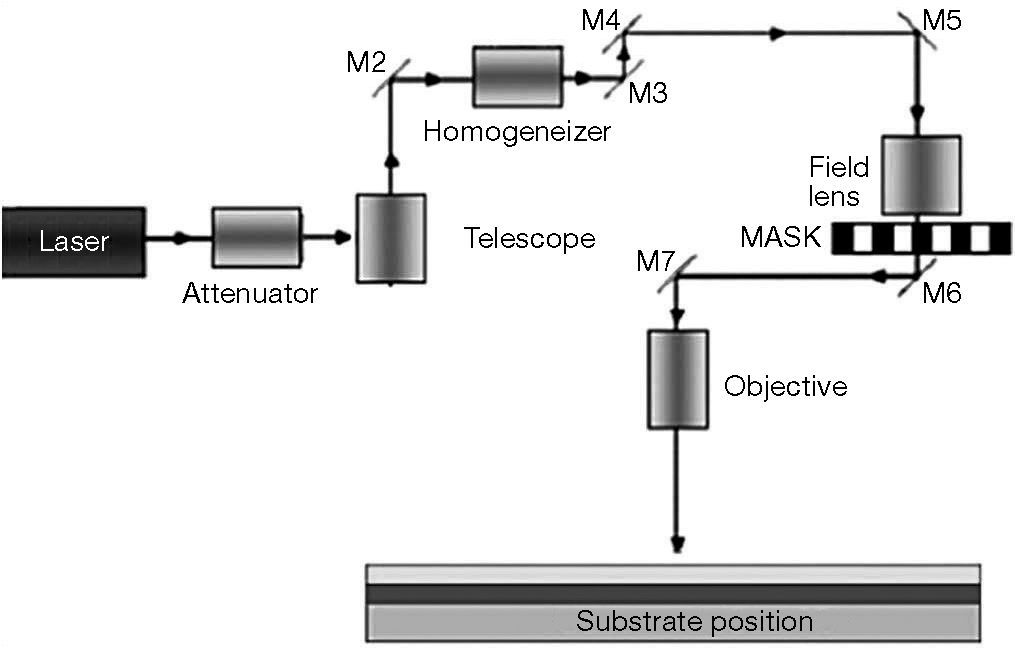
2Experiment2.1IZO thin film preparationHeading: numbered sequentially in Arabic numerals, left justified, in 10-point Arial Italics font, upper and lower case letters. The sol-gel precursors of IZO were prepared following the procedure described in Choi's work (Choi, Seo, & Bae, 2008). The synthesis flow is shown below. First, 0.1M of indium acetate [In(OAc)2] and 0.1M of zinc acetate dihydrate [Zn(OAc)2•2H2O] were dissolved in 2-methoxyethanol. Because of the limited solubility of Zn(OAc)2•2H2O in alcohols and the non-soluble property of In(OAc)2 in 2-methoxyethanol; 0.4M of diethanolamine and 0.4M of acetylacetone served as a stability agents and were added to 2-methoxyethanol solution for dissolution and the formation of a stable sol. Finally, the solution mentioned above was mixed at 60°C and stirred for 24 hr. IZO thin films were deposited on a glass substrate by the spin coating method. After the coating process, the wet thin films were dried at 300°C for 30min on a hot plate. In contrast to previous studies, the high temperature IZO annealing process was replaced by KrF excimer laser irradiation in which laser wavelength, fluence and shot number were 248nm, 300 mJ/cm2 and 5, respectively. To determine the process temperature, thermo gravimetric analysis (TGA) was performed under atmosphere pressure at a heating rate 5°C/min. The amorphous character and thickness of IZO thin films were confirmed by transmission electron microscopy (TEM). The sheet resistance of the thin film was measured by a high resistivity meter. The experimental setup for the laser annealing is shown in Figure 1.
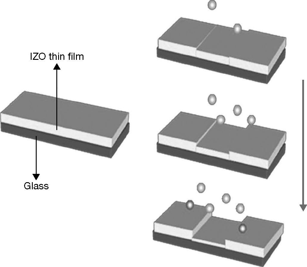
2.2Laser annealing in IZO TFTFigure 2 shows the Laser annealing process of the IZO thin film film. There are two process changes in our laser treated IZO TFT.
Step 1. Pre-baking time increasing. We keep the pre-baking temperature at 300°C, but increase the pre-baking time from 10min to 60min that could drive the undesired materials out.
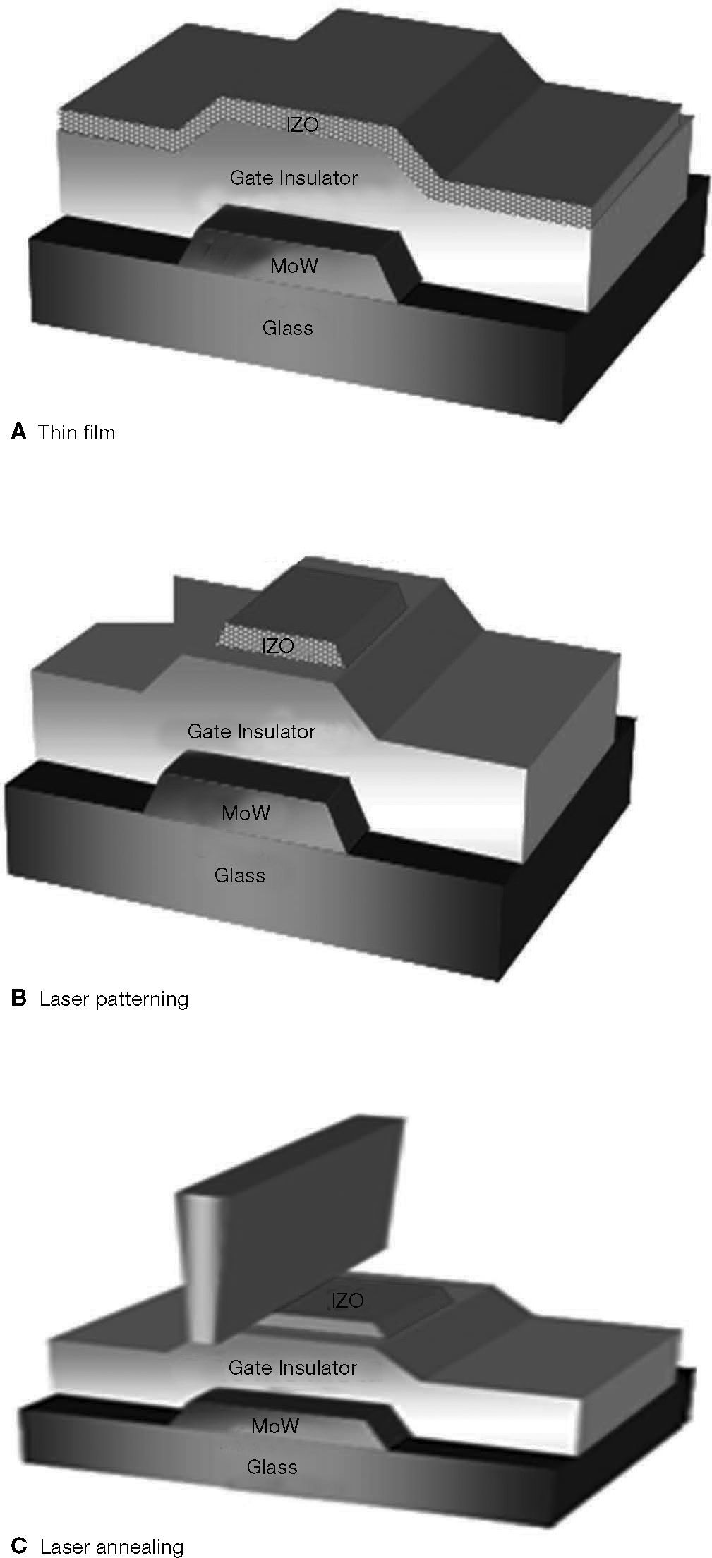
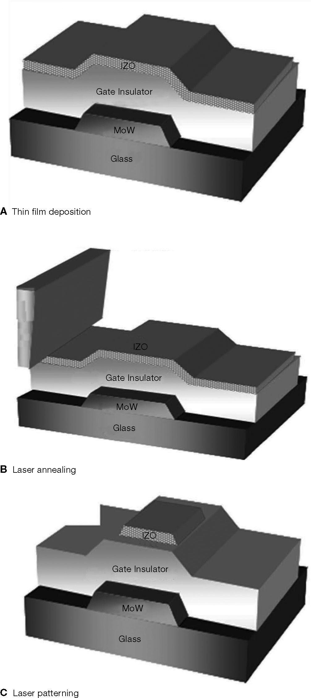
We would change the process flow of (A) island patterning_annealing to (B) annealing_island patterning as shown in Figure 3 and Figure 4. In our experience, the TFT with process (B) shows a better performance than that with (A).
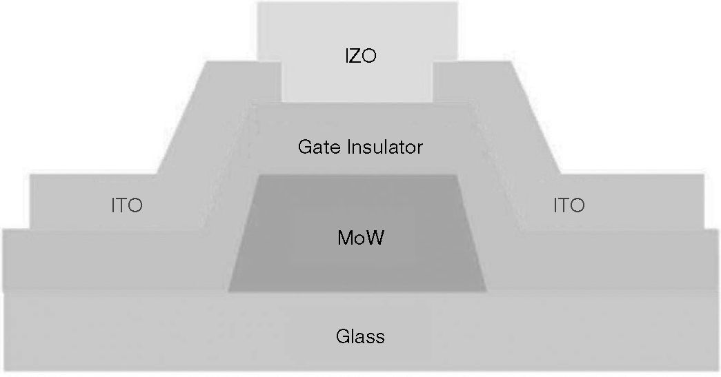
For the fabrication of IZO-TFT, a non-alkaline glass was used as a substrate. First, 100nm thick MoW was deposited by sputtering and patterned as a gate electrode. SiNx:H and SiOx with a thickness of 300nm was deposited by plasma-enhanced chemical vapor deposition (PECVD) as the gate insulator layer. Then, an IZO channel layer was deposited by spin coating, patterned by a photolithography and wet etched with diluted oxalic acid, and then annealed by excimer laser. Finally, sputtered ITO was deposited to form the source and drain electrodes. Figure 5 illustrates the schematic view of the IZO-TFT with bottom gate top contact structure.
3Results and disscussionsAll the electrical stability of IZO-TFT devices under gate bias stress was also investigated. In order to separate bias effects from light induced shifts of threshold voltage, all samples were measured in the dark at room temperature. The applied bias was 20 V to gate and the bias stress was interrupted at 10, 100, 1000, and 10,000 s in order to measure the transfer characteristics.
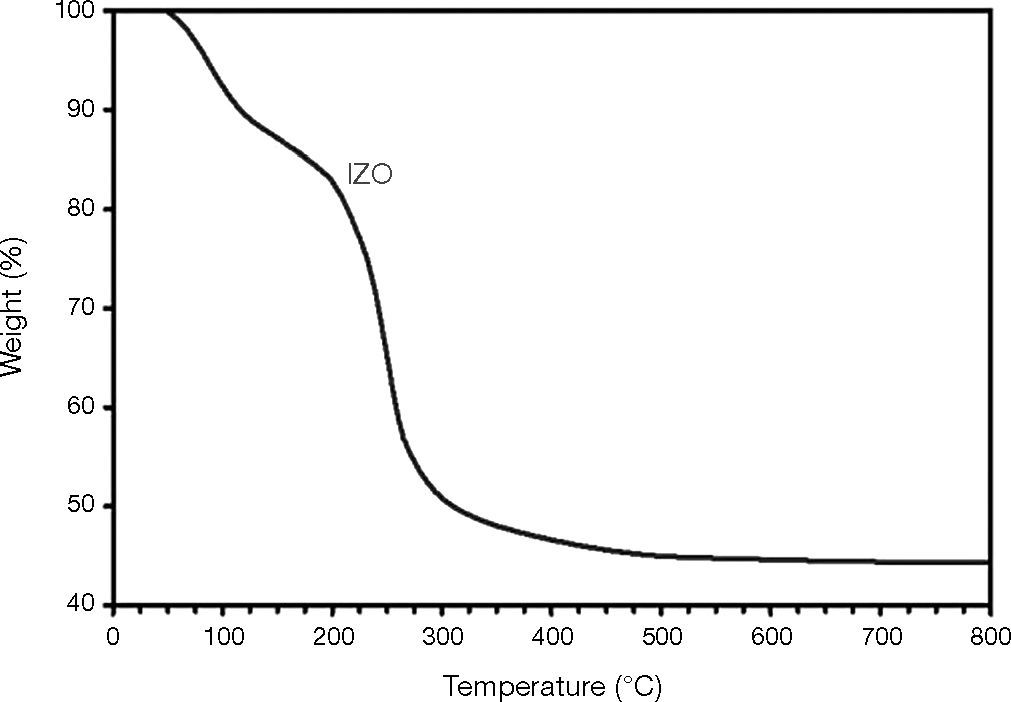
Figure 6 show the thermo-gravimetric analysis (TGA) curves of the IZO solution under a heating rate of 20°C/min from 50°C to 800°C. For the IZO TGA curves, three temperature regions of weight loss were observed at 50 ∼ 150°C, 150 ∼ 300°C, and 300 ∼ 400°C. When the temperature was higher than 450°C no obvious weight loss was observed. The TGA curve shows that the annealing temperature of 450°C could decompose all the organic compounds and form the IZO thin films. In addition, the suggested heat-treatment temperature was also obtained at 500°C from the TGA curve.
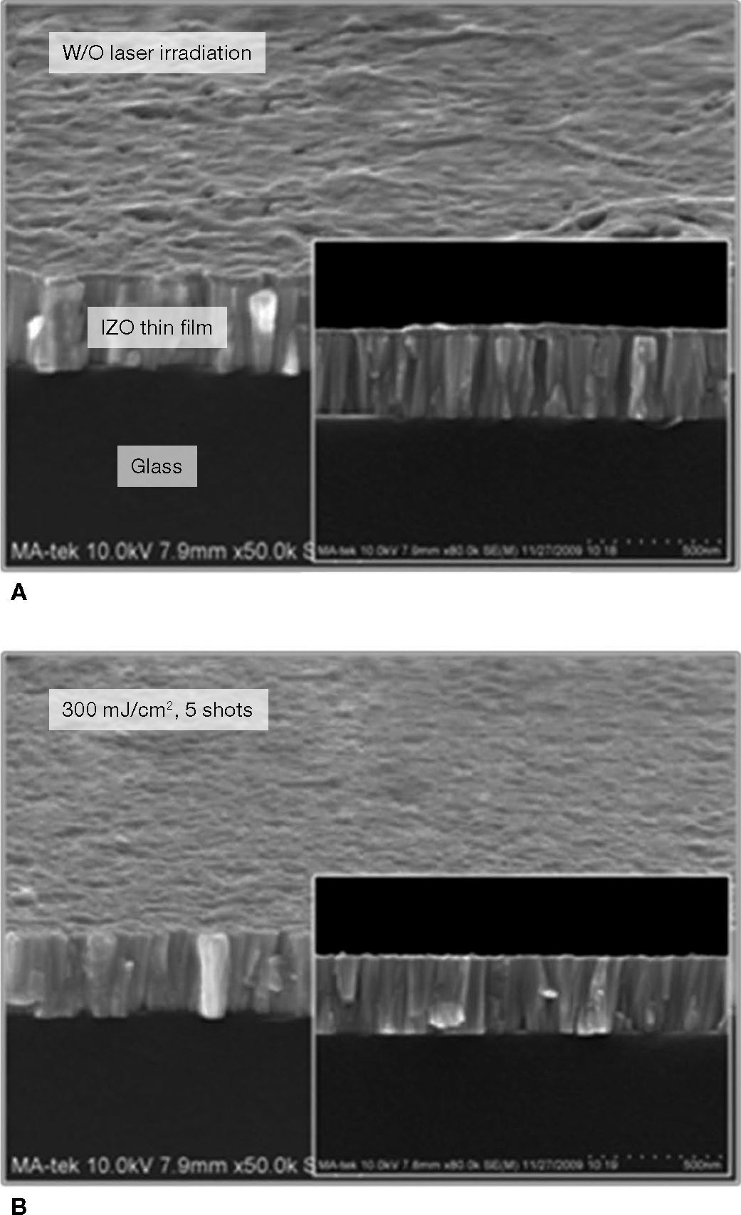
Figure 7 shows the SEM micrographs of 30-nm-thick IZO thin film (a) without laser annealing, (b) at a laser energy density of 300 mJ/cm2, with five shots. These results indicate that when the laser energy density is 300 mJ/cm2, the IZO thin film is still smooth and uniform. It can be seen that a film suffering laser annealing also keeps an uniform film quality.
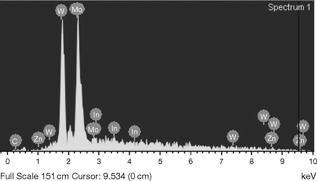
Figure 8 shows the energy-dispersive X-ray spectroscopy (EDS) analysis results for IZO with a KrF laser (300 mJ/cm2) annealing area. This should give a good indication of the IZO thin film chemical composition after laser annealing.
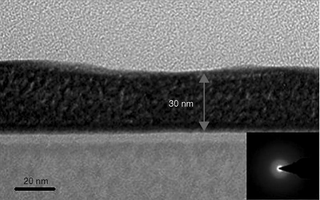
The IZO thin films showed an average thickness of 30nm as measured by transmission electron microscopy (TEM), as shown in Figure 9. From TEM diffraction, it can be seen that a film suffering laser irradiation also keeps an amorphous film quality.
The sheet resistance and resistivity of the films are 1.63×10¹² Ω/cm and 1.22×10⁷ Ω/cm, respectively. The resistivity value indicates that the deposited thin film is in the semiconductor range. IZO-channel devices with various gate insulators showed well-behaved TFT characteristics. The channel length (L) and width (W) of the IZO-TFT are 50 μm and 500 μm, respectively
The a-IZO TFT behaves as an n-channel transistor and exhibits good linear/saturation behavior. The electrical parameters were determined from a plot of Ids1/2 vs. Vg on the basis of the following relationship in the saturation regime: where Ids is the drain current, W and L are the channel width and length, respectively. Ci is the capacitance per unit area, μsat is the field-effect mobility, and Vth is the threshold voltage.
There are two process changes in our laser treated IZO TFT. We keep the pre-baking temperature at 300°C, but increase the pre-baking time from 10min to 60min that could drive the undesired materials out.
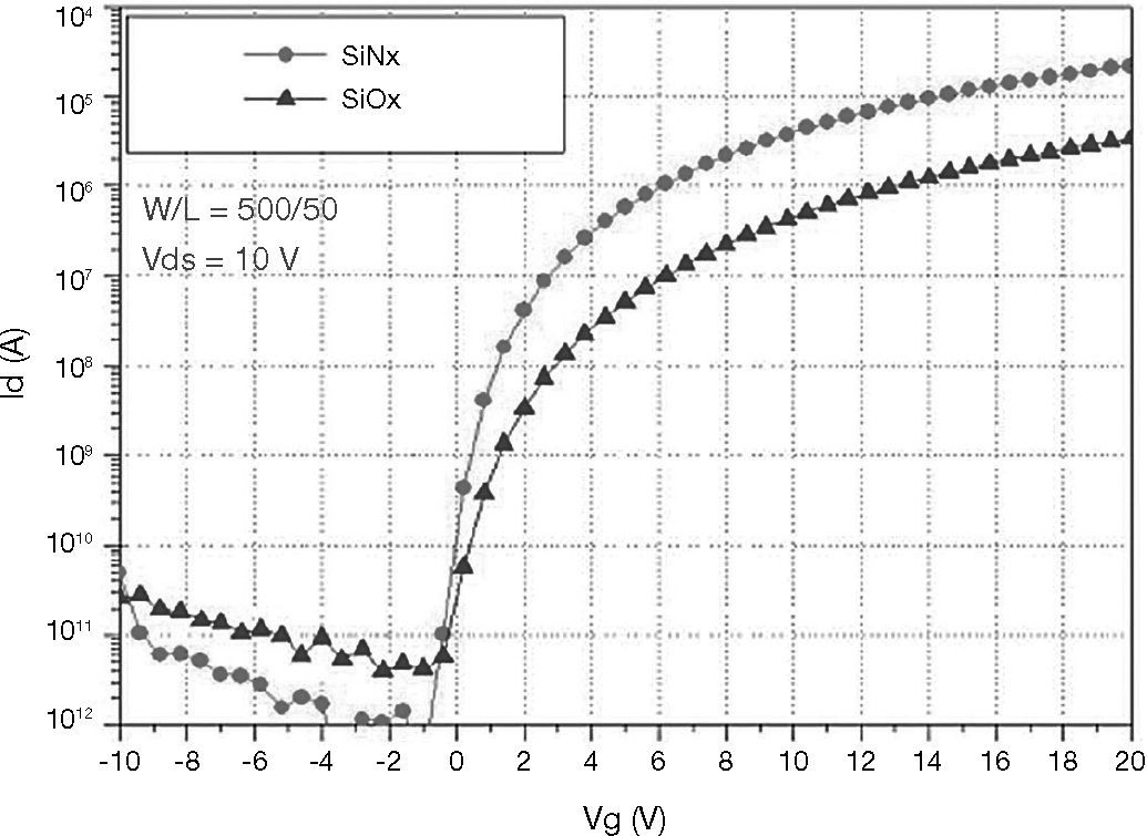
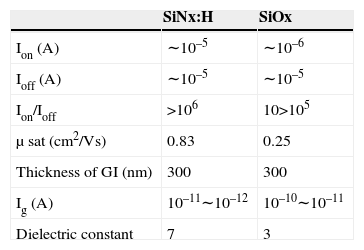
Like other ZnO-based semiconductors, IZO is n-type, and electrons are induced in the channel by the positive voltage applied to the gate. A comparison of the transfer characteristics of IZO-TFT fabricated with various gate insulators are shown in Figure 10. Relevant electrical parameters are summarized in Table 1. The off current of IZO-TFT fabricated with the various gate insulators are all in the region of 10–10∼10–12 A. The low off current is attributed to the fact that the IZO thin film is thin, amorphous and possesses a low intrinsic free carrier density, preventing bulk conductivity through the IZO semiconductor.
For IZO-TFT, the on/off ratio of the current is >105, which indicates that the IZO-TFT is applicable as an AMLCD pixel switch. The gate leakage current of SiNx:H and SiOx are also listed in Table 1. For the SiNx:H and SiOx, the leakage currents seem to be acceptable and both values are about 10–11∼10–12 A and 10–10∼10–11 A, respectively. The result shows that the SiNx:H and SiOx had good insulating properties and are suitable for application as a gate insulator.
Figure 11 shows the effect of applying a gate bias stress of 20 V to the gate of an IZO-TFT. For the devices with SiNx:H and SiOx gate insulators, as shown in Figure 11 (a) and (b), it is observed that the drain current-gate voltage (Id-Vg) curve shifts in the positive Vg direction with increasing stress time. This phenomenon suggests that electrons are temporarily trapped in the gate insulator or semiconductor or at the channel/insulator interface at pre-existing traps during the period of stress. With increasing stress time more holes and electrons are induced at the dielectric and channel, respectively. A negative gate voltage is needed to deplete the electrons in the channel of the IZO-TFT and fully “turn off” the device.
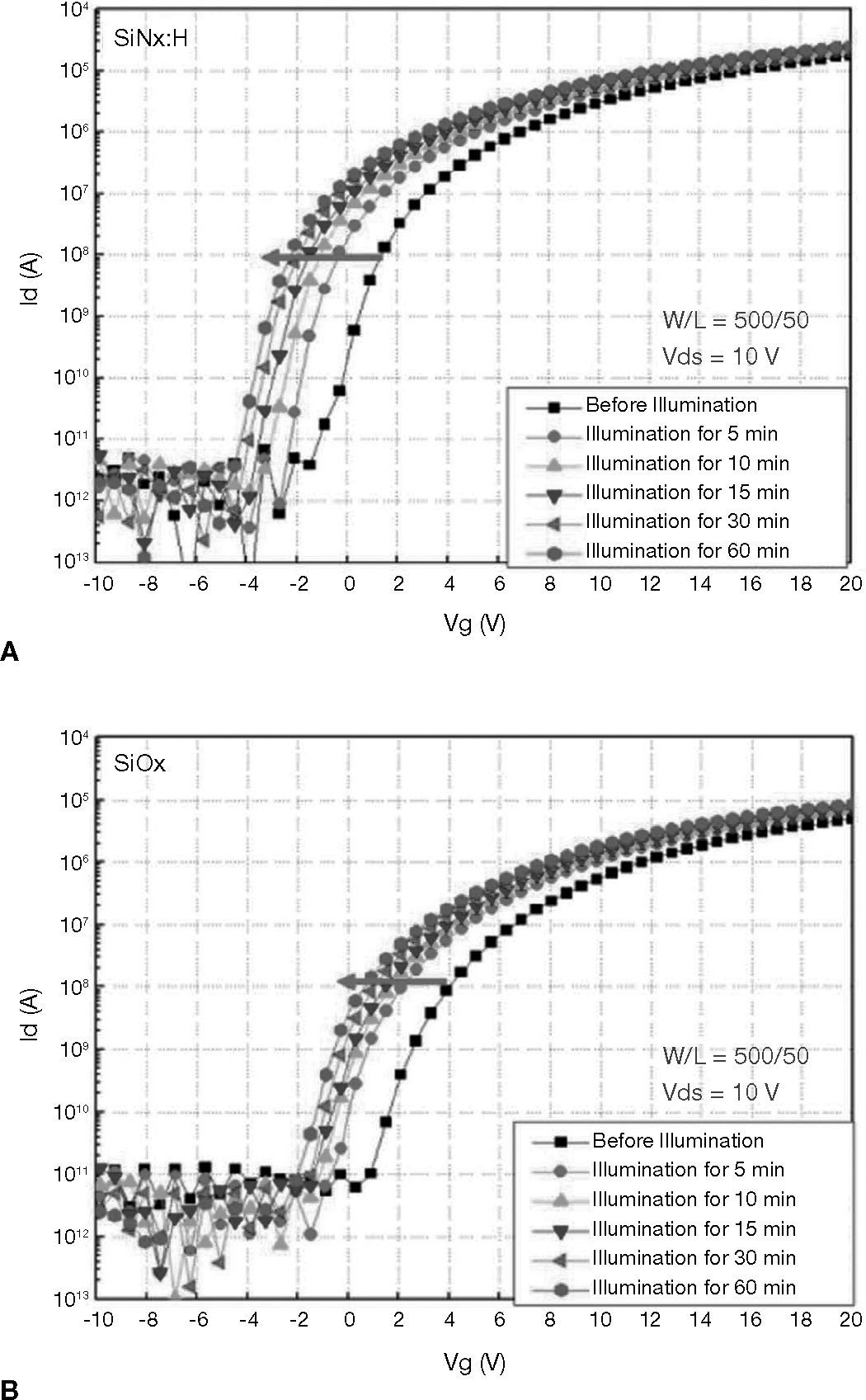
The transfer characteristics of TFT devices under illumination are presented with increasing illumination time. For the three devices, SiNx:H and SiOx, the original mobility and threshold voltage are 0.58cm2/Vs, 2.84 V and 0.33cm2/V, 3.78 V respectively. However, after illumination for 1 hour, the mobility and threshold voltage are changed to 0.52cm2/V, –1.43 V and 0.34cm2/V, –0.70 V. These results indicate that, during illumination, persistent photo carriers are generated in the IZO thin film, and IZO-TFT were shifted to depletion mode operation. The observed threshold voltage shift could be eliminated by baking at 150°C on a hot plate for 30minutes.
In the Figure 12, in all cases the Id-Vg curves shift to more negative Vg values. The output and transfer characteristics of IZO-TFT were measured in the dark at room temperature using the Keithley 4200-SCS semiconductor characterization system. The effect of light irradiation on the TFT transfer characteristics was analyzed with a Vds = 10 V and Vg swept from –10 V to 20 V. Illumination was provided by a xenon lamp with a luminance of 960 lux, measured by an luminance meter at room temperature.
4ConclusionsIn this study, IZO-TFT fabrication with a solution process and annealing by using KrF excimer laser has been investigated. Solution-processed IZO-TFT with SiNx:H and SiOx gate insulator were fabricated on glass substrates. Compared with the traditional process, the maximum process temperature can be as low as 300°C. In addition, the electrical stability and operation under illumination effect of the IZO-TFT devices with different gate insulator were also presented in this article. Solution based with KrF excimer laser annealing IZO-TFT device is applicable as an AMLCD pixel switch. In the future, this technology would be introduced in large-area flexible display.
The authors would like to thank the Asia University for financially supporting this research under contract No. 102-asia-37.


