This paper presents the methodology used for a digital integrated circuit design that implements the communication protocol known as Serial Peripheral Interface, using the Alliance CAD System. The aim of this paper is to show how the work of VLSI design can be done by graduate and undergraduate students with minimal resources and experience. The physical design was sent to be fabricated using the CMOS AMI C5 process that features 0.5 micrometer in transistor size, sponsored by the MOSIS Educational Program. Tests were made on a platform that transfers data from inertial sensor measurements to the designed SPI chip, which in turn sends the data back on a parallel bus to a common microcontroller. The results show the efficiency of the employed methodology in VLSI design, as well as the feasibility of ICs manufacturing from school projects that have insufficient or no source of funding.
En este artículo se presenta la metodología usada en el diseño de un circuito integrado digital que implementa el protocolo de comunicación denominado Interface de Periféricos Serial, utilizando el sistema CAD Alliance. La finalidad es mostrar cómo la tarea del diseño VLSI puede ser realizada por estudiantes o profesionistas, con un mínimo de recursos y experiencia. El diseño físico fue enviado para su fabricación usando el proceso CMOS AMI C5 caracterizado por un tamaño de transistor de 0.5 micrometros, auspiciado por el programa educativo de MOSIS. Las pruebas se realizaron sobre una plataforma que transfiere los datos desde mediciones de un sensor inercial hacia el chip SPI diseñado, el cual a su vez envía los datos de nuevo por un bus paralelo hacia un microcontrolador común. Los resultados mostraron la eficacia de la metodología de diseño VLSI empleada, así como la factibilidad de fabricación de diseños realizados en proyectos escolares cuyas fuentes de financiamiento sean insuficientes o nulas.
Nowadays, there are sophisticated commercial computer aided design (CAD) tools for professional use in the design of integrated circuits (IC) with very large scale integration (VLSI) (Weste et al., 2011). Examples are Cadence Design System, Synopsys and Mentor Graphics among others that require the payment of annual licenses. In public education institutions, the cost of software licenses becomes a limiting factor as well as the fact that their use is complex by novice designers.
The design process begins with the specification of a digital system and its description through a hardware description language such as VHDL (very high speed integrated circuit hardware). Once the behavioral description of a digital system design has been coded in VHDL, the software tools that allow synthesis and verification to obtain the physical plane of the IC are deployed (this process is known as flow design). Subsequently, the physical planes are generated in digital files that are sent for fabrication.
Students, professors and researchers that carry out VLSI design can use the software tools that allow the design flow of VLSI ICs in their studies and research projects because the learning curve is short. Alliance CAD System is the name of a complete set of CAD tools and VLSI design libraries that were developed in the Pierre et Marie Curie laboratory in Paris, France. Alliance is an environment friendly CAD system licensed under GPN Linux (LIP6, 2014; Silva, Yoshida, & Palacios, 2006). This software allows the design and test of VLSI circuits, from the specification to the physical layout, providing libraries of cells that allow the design of independent circuits specific to the technology used in the manufacturing process.
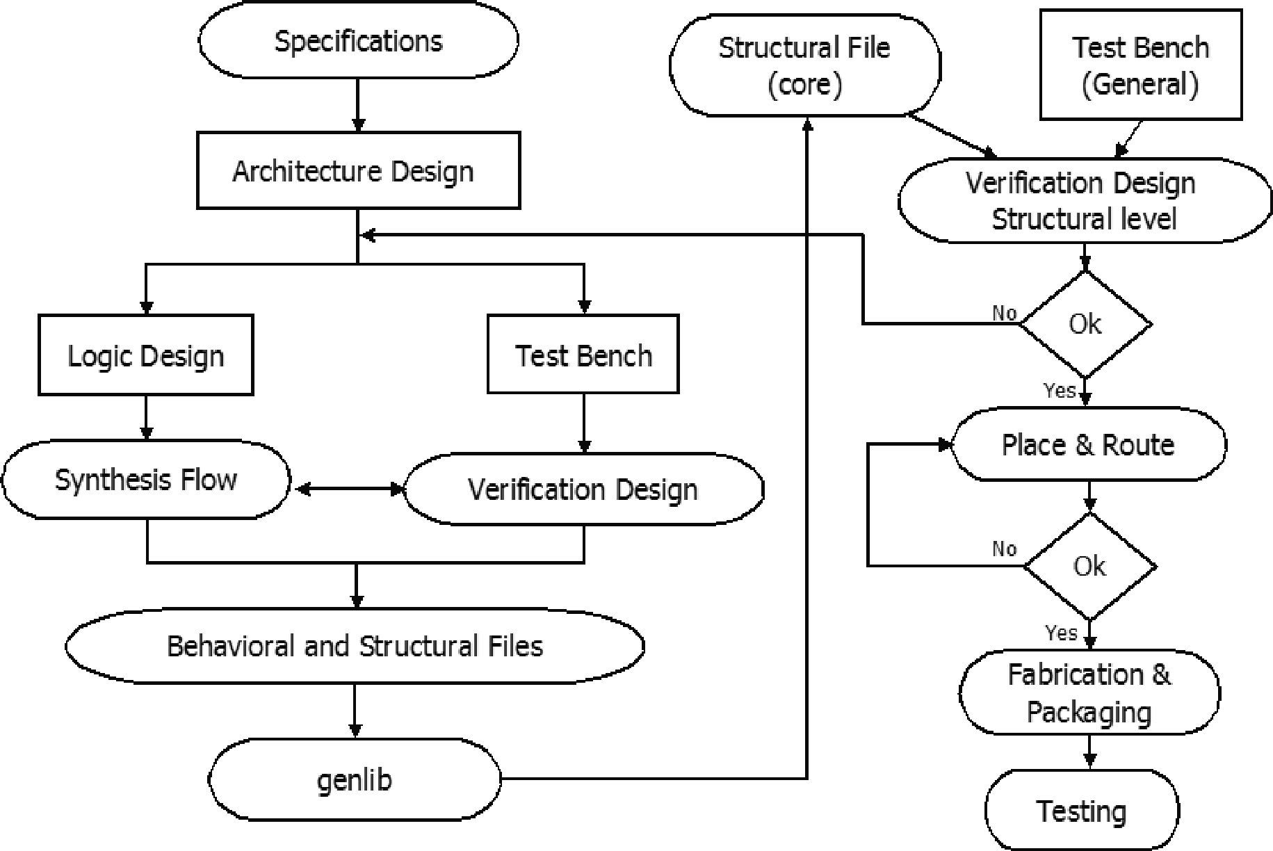
In this paper, the design methodology uses the Alliance CAD System tools for the design of a VLSI IC and is exemplified by the implementation of a communication protocol. Figure 1 shows a diagram of the method implemented in the design flow (Ortega, 2009; Reyes, 2011). The manufacturing stage and packaging was made through the MOSIS Educational Program (MEP) (Piña, 2002). The MOSIS Service (or MOSIS) provides manufacturing services at no cost to educational institutions with minimum financial support for non-profitable applications (Staudhammer, 1997; The MOSIS Service, 2014).
This paper is organized as follows: first, the specification of what the chip must do is presented. Second, an architecture design of the entire system in a hierarchical way is proposed. Third, the logic design is developed in a hardware description language. After that, the synthesis flow of the Alliance CAD tools is used. Then a test bench was prepared for verification design, followed by the place and route stage that was validated with the Alliance CAD tools before generating layouts files in a standar CIF format. Once the design was completed, it was sent for fabrication and packaging using the MOSIS Educational Program. Experimental testing was made for the chip using specialized citcuitry. Finally conclusions on this work are provided.
SpecificationsThe SPI protocol is a four-wire serial peripheral device that features a synchronous and bidirectional (full duplex), communication standard developed by Freescale (Leens, 2009). It is used to communicate microcontrollers with a variety of peripherals (A/D, EEPROMS, sensors, among others). SPI is a standard used to control almost any digital electronic device that accepts a serial bit stream controlled by a clock. It uses the following signals: Data In, Data Out, Clock and Chip Select (CS) or Enable. Some microcontrollers might use terms such as Master-Out-Slave-In (MOSI) or data from master to slave and Master-In-Slave-Out (MISO) or data from slave to master and Slave Select (SS) or slave selector.
This paper implements a SPI module with the main functionality of the SPI communication protocol. The module operates in master mode, and allows the user to configure the chip select signal (CS), clock polarity control (CPOL) and the data transfer frequency (SCLK) with up to 16 selection modes. The SPI module transmits/receives data frames of 16 bits, with the most significant bit of each word transferred first. The module is flexible enough to communicate with standard peripherals from various manufacturers that incorporate the SPI protocol.
Features:
- •
Master mode
- •
Chip select: active high or active low selection
- •
Full-duplex communication
- •
SCLK clock polarity selection: active high or active low
- •
Clock phase (CPHA): mode 1 is default
- •
16 frequency setting modes: divider between 2, 4, 8, 16, ..., 65536
- •
Data frames of 16 bits
- •
One peripheral in slave mode
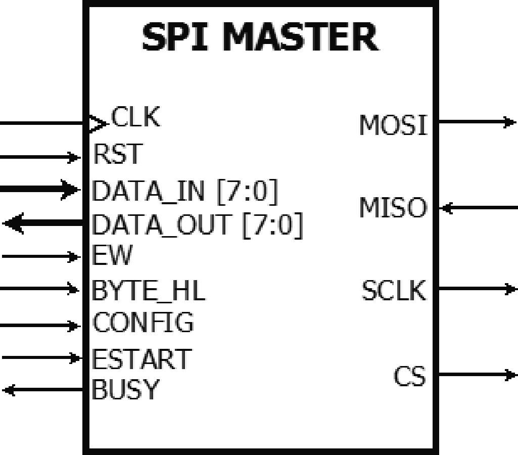
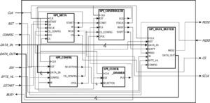
The design of the architecture of a VLSI digital integrated circuit begins with the development of the idea of the main module that will be called core. Followed by the definition of the module in terms of inputs, outputs, and a description of the specific function. Figure 2 shows a general diagram of the SPI MASTER. Table 1 describes the I/O terminals. In Figure 3, the modules SPI META, SPI CONFIG, SPI CONTROLLER, SPI CLOCK DIVIDER and SPI DATA BUFFER define the architecture of the SPI MASTER core.
Terminal description.
| Terminal | Type | Description |
|---|---|---|
| CLK | Input | Clock oscillator with a maximum frequency of 25 MHz |
| RST | Input | Performs a reset on the system |
| DATA_IN | Input | Input data bus (8 bits) |
| DATA_OUT | Output | Output data bus (8 bits) |
| EW | Input | Enables writing of internal registers |
| BYTE_HL | Input | Select the upper or lower byte from the 16-bit registers |
| ESTART | Input | Start the transmission/reception between the SPI Master and Slave |
| CONFIG | Input | Enables the configuration parameters required for the Master module |
| BUSY | Output | Reports that the module is busy |
| CS | Output | Enables communication between the SPI Master and Slave module |
| SCLK | Output | Clock between SPI Master and Slave module |
| MOSI | Output | Output serial data bus of the SPI Master |
| MISO | Input | Input serial data bus to the SPI Master |
The SPI Master core requires that the external signals be stable and synchronous during internal communication, therefore this module is necessary to prevent metastability problems (Wakerly, 2006). The input signals that require synchronization with the clock signal are ESTART and EW, generating the START, W. On another hand the signals ESCLK and ECS are passed trough D-Flip-Flops inside the SPI_META Module before be sended to the Slave device as the SCLK and CS signals. This is required in order to eliminate the transitory glitches that ESCLK and ECS could have, ensuring that the logic levels of SCLK and CS is stable along all the complete clock period (Wakerly, 2006).
SPI CONTROLLER ModuleThe SPI CONTROLLER module is responsible for producing the control signals (ECS ESCLK, BUSY and SHIFT) in the correct sequence in order to run processes with the required timing. The module consists of a main state machine that provides the inputs and outputs to multiple threads and it is constituted of two nested state machines that perform low-level processes.
SPI CONFIG ModuleThe SPI Master core requires a number of configuration parameters to perform its functions. These parameters are stored in a register within the configuration module namely:
- •
Setting the frequency of the SCLK output signal
- •
Setting the active level of the chip select signal (CS)
- •
Setting the polarity (CPOL) for the SPI bus clock (SCLK)
The SPI CLOCK DIVIDER module is designed to provide up to 16 clock modes as desired. The frequency division factor is defined by the SELECTOR bus signal.
SPI DATA BUFFER ModuleThis module contains the 16-bit register called REGISTER_DATA. It is intended to store the data to be transferred by the MOSI signal, as well as to receive the data from the MISO signal during the transmit/receive operation. This way, the data can be read from the output data bus (DATA_OUT) when the core finishes the transfer between the SPI Master and Slave module.
Principle of operationThe SPI Master core operation begins by enabling the RST signal and allowing the system to start with specific initial conditions. Subsequently, the core performs a one-time setup process and, followed by a cyclical writing, transmission-reception and reading.
The configuration process starts with the definition of parameters such as CS=0, CPOL=1 and SELECTOR=0x0. In this example the setting data will be equal to 0x20. To perform this configuration, the data are set in DATA_IN bus, after that, the CONFIG signal is set high, and finally the EW signal is set high, only under this condition, the chip is already configured and it is ready for the cyclical of writing-transmit-receive-reading process.
The writing process starts when the CONFIG signal is disabled, thus the first byte enters in DATA_IN to be written in REGISTER_DATA depending on BYTE_HL signal and if EW signal is enabled. For example, maybe we need the address 0x0007 be the data stored in REGISTER_DATA which will be sent by the MOSI line. Once the data is in the register, the transmission-reception process can begin. This process starts when the ESTART pulse is enabled, after that, SCLK, CS and BUSY signals are enabled, in addition to sending the data by MOSI and, simultaneously, receiving data from the MISO line.
The reading process is initiated when the BUSY signal is disabled, thus the controller can perform the reading of data stored in REGISTER_DATA through the DATA_OUT bus. Reading is performed by setting BYTE_HL signal high or low, depending on the required byte to be read.
Logic designHaving defined the architecture, the next step is the logical description through a hardware description language (HDL), which describes the operation of a digital logic circuit. VHDL and Verilog are the standard languages for logical description of an integrated circuit. The logical design describes the interconnection topology between gates and data transfer between registers. The result of the logical design is a text file in HDL code. This file contains a structural description of a module that is required to carry out the synthesis flow from a logic level to a physical level. The following logical description in VHDL shows the metastability module. For simplicity, only the signal EW is described. The code has two main sections: entity and architecture. The types of the I/O signals are described in the entity section. The architecture section describes the module by its behavioral way. For more information about VHDL refer to Mealy et al. (2013).
The synthesis flow of Alliance CAD System (Lam, 2004a,b,c) begins by using sources of behavioural VHDL files to get structural VHDL files deploying automated synthesis tools; in this case tools such as vasy, boom, boog and loon are used for optimization in synthesis and verification. During this phase, the verification stage is assisted by simulators that allow checking for errors. The SPI Master core is developed under a hierarchical or modular structure, such that each module needs to be independently verified and synthesized as outlined below (Reyes, 2011). Once both the structural and behavioral files for each module are available, the next step is the integration into a single structural file. In this case the genlib tool provided by the Alliance developers (Chaput, 2002) is used. In this step a vector file with test patterns should be prepared to perform the simulation and verification used for the behavioral validation of the complete core. The next step in the flow is known as place and route, here the synthesis software transforms the logical design to a physical design. In the place phase, standard cell libraries components are placed on transistor level, and therefore, in the route phase electrical connections are made between them. During this process, there are other phases for optimization of delays and a consumption of area. The result of the synthesis is a structural file named netlist, containing the list of cells and macros, gates and interconnections between them.
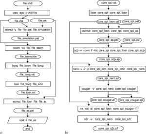
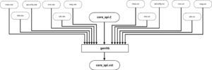
Behavioral and structural synthesis of the modulesFor synthesis of the SPI Master core, two processes are necessary since this design is performed in a hierarchical manner. Each module is an independent design in a hierarchical level. The first process is to synthesize each module individually in order to obtain the behavioral files (vbe files) and structural (vst files) used for the structural synthesis of the entire core. The design flow used for the synthesis of each module is shown in Figure 4a (Ortega, 2009), where the following structural files were obteined: meta.vst, clkd.vst, spiconfig.vst, sme.vst, sdb.vst and meg.vst. Once the synthesis of each module has been performed, one must continue with the flow of figure 5, using genlib, which is a circuit description tool that includes a set of functions in the C programming language. To generate the structural core_spi.vst file, firstly a text file with a .c extension must be edited. This file will be the input file to the genlib tool. Finally, Figure 4b shows the structural synthesis flow, placement and routing the SPI core layout in order to obtain the CIF file used for manufacturing.
Test BenchIn order to verify that the logic design complies with the desired function, a number of test pattern files must be prepared. The test files contain the expected response to an input stimuli sequence. This stage of the design cycle is critical and requires careful definition of the test patterns to ensure that the system responds correctly in every state for any stimulus applied. I/Os representing the SPI core functionality are defined in the stimuli file, in our case core_spi.pat. The writing of the stimuli file is a very time consuming activity. However the tool genpat undertakes this work in a procedural way. In (Lam, 2004a) tutorial part 1, more information on genpat can be found.
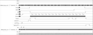
Verification designThe stimuli files must contain the inputs and outputs of the module to verify. This step is carried out with a tool called asimut. In the synthesis flow, asimut is used at different stages, since it is necessary to verify each module independently. Finally, a complete verification of the core is necessary to identify errors before sending the design to fabrication. The behavioral validation stage is essential; it may represent more than 70% of the effort devoted to the design of the chip. Simulation results of the SPI Master core are shown in Figure 6. It can be seen that the proposed design perfomes appropriately.
Place & routeAt this stage of the design process the layout plane must be prepared (Figure 7). The ocp tool performs automatic placement of standard cells. The nero tool traces the interconnections between transistors. A tutorial can be found at (Lam, 2004). With the cougar tool, extraction parameters of transistors and capacitances of the core can be obtained. The lvx tool performs a structural comparison of the extracted file against the original .vst file to verify that the obtained core layout meets the initial specifications. This comparison is called Layout vs Schematic. The obtained core contains a total of 3,477 transistors and its dimensions are 586 x 1451 lambdas (symbolic units). Figure 7b shows the view of all the layers of the design set by Alliance. Before sending the design to fabrication it is necessary to perform a scaling process into the chosen technology. In this step the s2r tool is used.
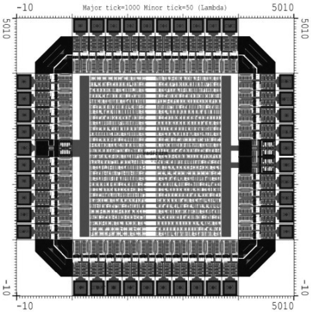
Padframe incorporation with the synthesis of the SPI Master coreIn order to have external access to the obtained core layout we must incorporate input and output pads around the core in a rectangular ring structure called padframe (Figure 8). In this padframe, the manufacturer makes the connections between the leads and the internal pins of the chip packaging. We can use the free software tool called Magic to place the padframe (Magic, 2013). Magic can also be used for the design rule cheking step (or DRC). With this step we check that the layout does not have violations of the design rules, in this way there is satisfactory confidence that the chip will meet the specifications once it is manufactured.
Fabrication and packagingThe step prior to sending the chip for fabrication requires the scaling of the layout to the selected process technology and the design rules checking for physical verification. There are two common ways to describe layouts: 1) the Caltech Interchange Format (CIF) which is used in universities, and 2) the Calma GDS II Stream Format (GDS) which is normally used in the industry. The final file of this work is a CIF file and it was sent to the MOSIS Educational Program, see (Piña, 2002; Staudhammer, 1997).
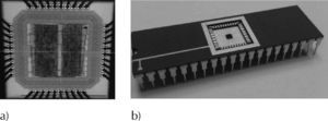
Experimental resultsThe SPI Master core was designed with the Alliance CAD System tools, by graduate students at the Centro de Ingeniería y Desarrollo Industrial in Querétaro, Mexico. Figure 9a shows a photo of the SPI Master core chip. The chip was sent for manufacturing in January 2013 using the services of the MOSIS Educational Program (MEP). Three months later, five chips were received. The process used was C5 in ON Semi 0.5 micron CMOS technology with a die size of 1.5mm x 1.5mm wired in a DIP40 package. This process requires the use of thin gold lines to connect the pads. The core die is placed in the center of the package. The wiring process was also carried out by MOSIS.
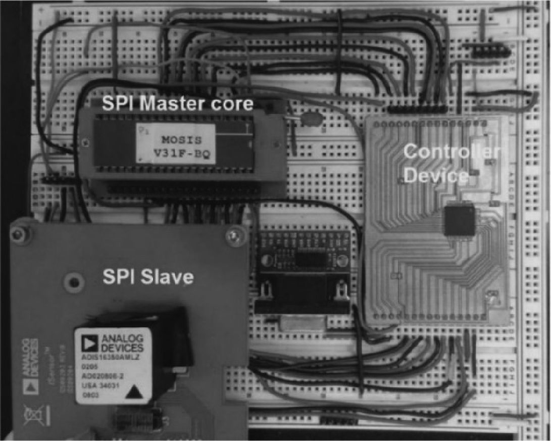
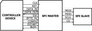
Once the chip was manufactured, tests and measurements were carried out. This ensured that all the design specifications were met and the chip worked properly. To perform the experiments with the SPI Master, a circuit that generated the control signals required by the chip was assembled. This circuit also set the data settings and the addresses that would be read from the slave device. Therefore the complete system test was made on a platform comprised by the chip SPI Master, the controller device, and an SPI Slave device, see Figure 10.
The tasks to be performed by the controller device were:
- a)
Generate the control signals {RST, CONFIG, EW, BYTE_HL, ESTART}, as required.
- b)
Set the setting data (6 bits) in DATA_IN master module.
- c)
Set the addresses (16 bits) as the SPI Master sends through MOSI signal.
- d)
Receive the BUSY signal.
- e)
Receive the BUSY signal, the controller could read data by the MISO signal. These data were read by the DATA_OUT in blocks of 8 bits.
The SPI Slave can be any device that sends information using the SPI communication protocol. In this work the ADIS16350 inertial sensor from Analog Devices was tested. The ADIS16350 consists of 3 accelerometers and 3 gyroscopes assembled orthogonally, with the following addresses: 0x0500, 0x0700, 0x0900, 0x0B00, 0x0D00 and 0x0F00. The operating frequency is defined in the range of 0.01 to 2MHz, the signal CS operates in active low and the polarity of SCLK active in high.
At this stage, the development of a platform to test the five chips was also part of the project. The platform generates signals that stimulate the chip (Figure 11). The SPI Master core processes genuine SPI information from the inertial sensor. This mechanism allows the evaluation of the signals generated as a result of interpreting the chip readings.
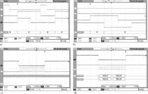
In order to describe the functional processes, an example of the results that were obtained in the corresponding experiment is presented. For the clock signal, a CLK frequency of 25MHz was set. The controller device generates an RST short pulse (green signal in figure 12a), then, the device starts the process of configuring the SPI Master core. The data configuration was established by writing a 0x20, signals CONFIG and W (red and blue respectively in figure 12a) are shown.
After configuring the SPI Master core, the writing process continues. In figure 12b, this process can be seen. The RST signal (green line) and CONFIG signal (red line) are disabled. The address to be sent by the MOSI line, corresponds to the sensor to be read; 0x0700 in this example. In order to write the most significant byte, the BYTE_HL signal (pink line) is defined high and W (blue line) is enabled in order to store the byte 0x07; subsequently BYTE_HL is set low and W is enabled to store the 0x00 byte. To start the process of transmission and reception shown in figure 12c, the START signal was enabled, and the process began by generating the CS signal (blue line in figure 12) and the clock interface of SCLK (red line in figure 12). Once the process is complete, data is available to be read via the MISO line. Figure 12d shows the obtained results. During this experiment, a 25MHz external clock is used (green signal in figure 12), the configuration parameter SELECTOR was changed and the SCLK clock frequencies obtained went from 125Hz to 4MHz.
ConclusionsA VLSI design methodology that allows the synthesis of a digital integrated circuit using a free CAD tool is presented. This methodology was evaluated by designing and implementing the SPI communication protocol in a chip designed by graduate students. The design was sent for fabrication using ON Semiconductor C5 technology, with support from the educational program sponsored by MOSIS. Five chips were received, and testing of every chip was carried out with an electronic platform that enables the transmission of data received from the inertial sensor through the SPI bus of the chip. The chip sends data back to the platform on a parallel bus to a common microcontroller for post processing of the data. Successful operations on every chip were observed. This proves the maturity of the manufacturing process and confirms the quality of the fabrication service offered by MOSIS at no cost to school projects. The results of the analyzed data are also useful to illustrate qualitatively the effectiveness of the proposed VLSI design methodology using the Alliance CAD tools.
Citation for this article:
Citación estilo Chicago
Chávez-Bracamontes, Ramón, Reyna Itzel García-López, Marco Antonio Gurrola-Navarro, Manuel Bandala-Sánchez. VLSI design with Alliance free CAD tools: an implementation example. Ingenieria Investigacion y Tecnologia, XVI, 03 (2015): 441-452.
Citación estilo ISO 690
Chávez-Bracamontes R., García-López R.I., Gurrola-Navarro M.A., Bandala-Sanchez M. VLSI design with Alliance free CAD tools: an implementation example. Ingenieria Investigacion y Tecnologia, volume XVI (issue 3), July-September 2015: 441-452.
The present work was supported by the Consejo Nacional de Ciencia y Tecnología, CONACYT, grant numbers 262864 and 262353. Also thanks to MOSIS that provided the manufacturing via the MEP program in partnership with the Centro de Ingeniería y Desarrollo Industrial under reference number 900452 and the authors that collaborated.
The VLSI design process with Alliance free CAD tools in education institutions has just a few requirements: an educational course involved in this research area, and minimum hardware and software for its implementation.
First, a VLSI design course covering the basics of electronics and computer science is needed. The background on CMOS devices and manufacturing technology, CMOS inverters and gates, propagation delay, noise margins, and power dissipation, sequential circuits, arithmetic, memories and design methodologies is necessary for understanding, designing, and optimizing digital circuits with respect to different quality metrics: cost, speed, power dissipation, and reliability.
A laboratory with access to computers or workstations is required to design VLSI chips. Alliance VLSI CAD Systems runs over Unix/Linux platforms, from i386 based microcomputers to SparcStations and DecStations. The software is registered under the GNU General Public License (GPL), so binaries, source code, and cells libraries are freely distributed. The packages are avalaible online from RedHat Entreprise Linux 6 (RHEL6) and clones (Scientific Linux 6, CentOS 6), Fedora and Ubuntu LTS distributions (LIP6, 2014).
Alliance VLSI CAD Systems provides some process independence in order to allow the designers to easily port their design from one technology process to another, this makes the design of circuits independent of the technology used in their fabrication step.
The following tools are used during the synthesis of VLSI digital circuits, for a detailed description see (Lam, 2004) and (Silva et al., 2006).
VASY (VHDL Analyzer for Synthesis). Converts a file written in VHDL VASY subset of the subset of VHDL Alliance.
BOOM (Boolean Minimization). Performs Boolean minimization on the incoming file written in the subset of VHDL Alliance. It is used in the first step of the synthesis process. Optimizes a behavioral description using reduced ordered binary decision diagram for the representation of logic functions.
BOOG (Binding and Optimizing On Gates). Boog is a mapper from a behavioral description into a library of standard cells as SXLIB. It is the second step of logic synthesis. Implements the input file, written in VHDL subset Alliance as a structural VHDL file where all entities used are contained in the specified cell library. The output file format is in VHDL structural Alliance.
LOON (Local Optimizations of Nets). Introduces some buffers to improve the current drive of some cells, but without modifying the original logic function. Both the input file and the output are written in VHDL structural Alliance. It is a CAD tool to remove problems and optimize FANOUT delay times, generating outputs with improved times.
ASIMUT (A SIMUlation Tool for hardware description). Behavioral and structural file format could be the input file for validate digital designs, attached to the subset of VHDL Alliance. But its most important use is to compare the input file against a test premade.
OCP (automatic tool for standard cell placement). Receives a structural VHDL file where all instantiated entities correspond to the previously indicated cell library.
OCP places the plane of each cell layout instantiated on a coordinate plane representing the surface of the chip. The output file does not yet contain information of interconnections but tries to place the cells subsequently interconnect as close as possible.
NERO (NEgotiating ROuter). This tool receives two files: one with extension .ap (generated by OCP) containing the cells positioned in the plane of the chip, and other with the .vst file (generated by LOON) containing the interconnections between the instantiated cells. Generates an .ap file containing cell layouts well positioned and the metal interconnections. The output file is the full layout in symbolic units.
COUGAR (Hierarchical Netlist Extractor). This tool is applied on the symbolic Layout file (extension .ap) produced by Nero Cougar and makes an extracting structural file extension (logical alliance) that subsequently was compared with the structural .vst produced by LOON.
LVX (Logical Versus eXtracted net-list comparator). Tool for comparing structural .vst and .al format files.
S2R. Tool to convert units in symbolic layout (.ap extension) to a layout in real units (.cif file extension). The CIF file layout in real units is to be sent to the manufacturer for construction.
Leens F. An Introduction to I2C and SPI Protocols. IEEE Instrumentation & Measurement Magazine, volume 12, 2009: 8-13.
Magic Development Team, Magic VLSI layout tool, version 7.5, 2013, [on line]. Available on: http://opencircuitdesign.com/magic/
Ramón Chávez-Bracamontes. BEng degree and MSc degree by Instituto Tecnológico de Ciudad Guzman (ITCG), Jalisco, Mexico, in 1991 and 2005, respectively. He is currently a PhD candidate in Science and Technology at the Centro de Ingeniería y Desarrollo Industrial (CIDESI) Querétaro, Mexico. He is a faculty lecturer since 1991 in several undergraduate and graduate programs for Electrical & Electronics Engineering, Mechanical and Systems at ITCG in several areas such as Power Electronics, Instrumentation, Digital Systems, Optoelectronics, Digital Signal Processing, Electronic Design, and Electrical Measurements.
Reyna Itzel García-López. BEng in Electronics Engineering by Instituto Tecnológico de Querétaro in 2011, MSc in Science and Technology with specialization in Mechatronics from CIDESI in 2013.
Marco Antonio Gurrola-Navarro. BEng in Electronics and Communications by Universidad de Guadalajara, Mexico in 1997, MSc in Earth Sciences by Universidad de Guadalajara, 2003, and PhD specialized in IC Design, by the Instituto Nacional de Astrofísica Óptica y Electrónica, in Tonantzintla, Mexico in 2009. Since 2009 he has been working at the Universidad de Guadalajara and is a member of the Department of Electronics at the Centro Universitario de Ciencias Exactas e Ingenierías, CUCEI. His research interests are design of digital and analog integrated circuits.
Manuel Bandala-Sánchez. BEng in Electronics Engineering by the Instituto Tecnológico de Puebla in 2001. MPhil / PhD in Microsystems & Sensors Engineering by the University of Lancaster (UK) in 2009. His professional experience includes companies/organizations like Centro de Ingeniería y Desarrollo Industrial (CIDESI, Querétaro), Hybrid Instruments (Lancaster, UK), Integrated Solutions Group (GSI, Puebla), Engineering and Instrumentation and Metrology Services (ISEYSA, Tlaxcala). His research interests are microsystems, microcontroller programming and MEMS.


