Semiconductor Laser or Light Emitting Diodes, (LEDs) as active elements of optical switches or spatial routing devices are widely used in integrated optical circuitry. Electro-optic, magneto-optic, mechanical or other methods are applied for that purpose. The present paper deals with a novel effect, which appears in the light field of a. c. driven luminescence emitters in Fabry-Perot structure under electrical excitation depending on time (a.c.), characterized because the light band emitted on the side face of the device moves up and down due to the finite diffusion velocity of the injected excess minority carriers. The combination of such emitter with a portioned detector element, allows spatial routing between these two detector segments. Particular emphasis is laid on a theoretical treatment of light propagation inside the emitter bulk which finally allows the construction of the light field intensity on the side face of the Fabry-Perot body, necessary to prove the proposed effect.
Láseres semiconductores o diodos fotoluminiscentes (LEDs) como elementos activos en switches ópticos o dispositivos de ruteo espacial son ampliamente usados en circuitos ópticos integrados. Para tal fin se aplica métodos basados en electro-óptica, magneto-óptica, mecánica, y algunos otros. En este trabajo se presenta un efecto novedoso, que aparece en el campo de radiación de diodos fotoluminiscentes en estructura Fabry-Perot bajo excitación eléctrica dependiendo en tiempo (a. c.), caracterizado por que la cinta de la luz emitida sobre la cara lateral del dispositivo se mueve hacia arriba y abajo debido a la velocidad de difusión finita de los portadores minoritarios inyectados. La combinación de tal emisor con un elemento detector partido permite el ruteo de la señal de luz entre estos dos segmentos del detector. Se pone particular énfasis en el tratamiento teórico de la propagación de luz dentro del volumen del emisor, que finalmente nos permite la construcción de la intensidad del campo de luz en las caras laterales del cuerpo Fabry-Perot, necesario para la comprobación del efecto propuesto.
The purely optical information transmission goes beyond any other means of data transfer given its enormous transmission rate capability up to terabytes per second at an extremely-low-energy consumption. Laser diodes and light emitting diodes are starting to compete in the field. The on-chip Light Emitting Diode (LED) allows to transmit ten Gbit/s and requires 2000 times less energy as the best actually used on-chip diode Laser [1, 2].
LEDs are used also as tunable electro-optic Fabry-Perot filters where a variable spacing between mirrors in a Fabry-Perot interferometer configuration allows for a relatively wide spectral tunability [3, 4]. The application of Laser diodes or LEDs as active elements in optical switches is common [5, 6, 7]. Such a device enables signals in integrated optical circuits to be switched from one circuit to another. To achieve this, several means are used, including mechanical, electro-optic, magneto-optic as well as other methods. A survey of routing methods in optical switching networks, and special components are discussed in recent publications [8, 9, 10]. In this article, we present a special effect, occurring in LEDs which has not yet been considered for routing applications.
The maximum of intensity of the near-field of a LASER-structure of Fabry-Perot type under a. c. or pulsed excitation in the spontaneous emission mode moves up and down on the side faces. This is due to the finite diffusion velocity of the injected minority carriers into regions of strongly changed optical absorption. The far-field behaves correspondingly, which allows the construction of a switching element, formed by the optical transmitter and a close-by sectioned detection element for spatial routing. We describe fallowing, the construction of the radiation field outside a Fabry-Perot type Laser structure in the spontaneous emission mode. The combination of such LED with a sectioned photodetector provides, in a straightforward manner, a spatial routing of an optical signal, which at the same time is reproduced with a phase difference on the two-detector elements.
Light emitting diodes are formed by a p-n junction in a semiconductor bulk. Considering as an example a classical GaAs-LED, the generated recombination radiation inside the p-n region suffers a more or less strong optical absorption on its way toward the emitting external surface. The graded doping of the p-region by over compensation of the otherwise n-type substrate in the diffusion process generates an optical absorption coefficient α(r→), which is a steep function of the coordinate perpendicular to the junction plane, while the absorption of the n-region maintains an almost constant low- absorption coefficient for the recombination radiation generated on the p-side of the p-n junction. This difference of the optical absorption together with the time-delayed recombination process of the proceeding minority carriers under pulsed-excitation due to the finite carrier mobility results in a light field outside the LED, whose intensity maximum moves slightly up and down on the face of the Fabry-Perot structure.
The propagation of light through an inhomogeneously absorbing medium, in which only the optical absorption α depends on the space-coordinates r→, exhibits interest in investigations of light emission and light propagation in solids. In the case of stratified media a number of investigations of wave-guiding [11-13] and beam focusing properties exist. For the description of laser operation in semiconductor p-n junctions, step like [14, 15] and continuously changing [16, 17] functions of the optical absorption α(r→) have been used.
In order to describe the spontaneous emission of a light emitting diode possessing a considerable variation of optical absorption along the current lines, the question of the validity of a ray-like description of the light propagation in such media appears. Therefore, we first investigated the solution of the wave equation by a ray-like light propagation process and corrections to this approach in Section 2. Then, the intensity of light of an emitting plane at the diode surface perpendicular to this plane is obtained in Sections 3 and 4. From it, the near-field intensity of a LED can be calculated. Finally, the time-dependent injection is discussed in Section 5.
2Propagation of recombination radiation in the approach of light raysIn order to describe the light propagation through inhomogeneously absorbing media, we start with the wave equation for harmonic oscillations
Where ψ(r→)denotes the r- dependent part of any component of the space-time dependent electromagnetic field vectors, Ω=k0n*is assumed to be constant, k0- wave number in vacuo, n*-refractive index, and αdenotes the r- dependent absorption coefficient.
We consider here the special case of a homogeneous refractive index, but an inhomogeneous absorption. Further we assume, that the atomic oscillations feel no anisotropy (as, e.g., birefringent crystals or at the diffraction of light by small particles) so that αand Ω are scalar quantities. Then the wave equation can be written down for the components of the electromagnetic field vectors separately.
In the concept of light rays, an approximated solution of the wave
Equation 1, can be obtained in the limit of small lengths, where k0 tends to infinity, we make for the solution of (1) the well-known statement see [18]
Where the eikonal S(r→) and the amplitude a(r→) can be expanded in powers of 1/k0 :
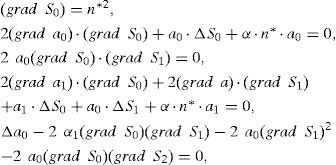
The function S0(r→), S1(r→), a0(r→) etc. fulfill the Equations
etc.
As a boundary condition we chose the form of a plane wave. Without any restrictions, we can take Ψ(z=0)=A. This means, the coordinate system is arranged in such a way, that the normal unity vector on this plane
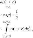
Ψ=const. shows into the z-direction. In this way, we obtain a solution of (4)
The normal unity vectors of the phase surface S(r→)=const. specify the direction of energy flux (n* is assumed to be scalar). This direction defines the direction of the light rays.
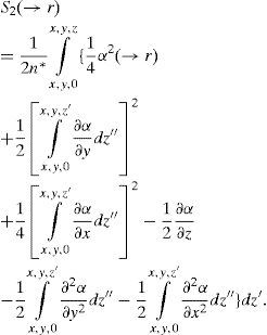
The expansion (3) corresponds to the transition from a wave-like to a ray-like description of light propagation. S0 designates a straight-on propagation through the medium, at which the intensity decreases like a02. The next term S2(r→) (8) corresponds to the first correction of the straight-on propagation.
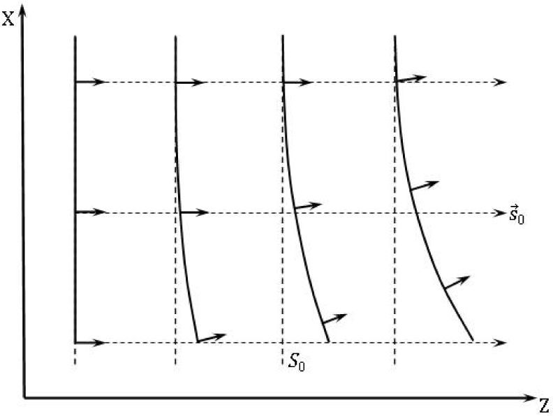
In general, the phase surfaces S(r→)=const. are bended. As example we consider a medium with an absorption coefficient α(r→)=βx. This yields in Figure 1. The light is diffracted into the region of higher absorption
In the same manner, a correction to the amplitude (6) can be obtained by solving the equation 2(grad a2) (grad S0)+(grad a0) (grad S2)+a0ΔS2+αn*a2=0
Next, we confine ourselves to the first-order approximation, i.e., we neglect the additional diffraction effect due to the wave nature light. This approximation is valid in the limit |grad α|/k0α<<1.
The concept of light propagation along light rays is less established if the properties of the medium vary strongly within the region of one wave length. In such case it is possible to describe the light propagation process by expanding the wave function with respect to a complete set of normal oscillation modes. This method is familiar from the description of a coherent emission of laser structures with similar absorbing properties, see, e.g., [18].
However, it is not expected that the wave field of a point source-is situated within an inhomogeneously absorbing medium-can be approximated sufficiently by using only a low number of oscillation modes.
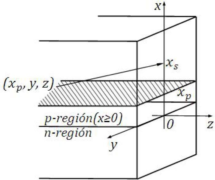
3Point emitter in an absorbing mediumLet us investigate the light propagation of a point emission source embedded in an
inhomogeneously absorbing medium (see Figure 2) with an absorption function given by
Such function is suggested for a p – n junction in GaAs diodes [16]. The sample is assumed to be cube like with an interface between the p and n region at x=0. The point source is situated at rp=(xp,yp,zp). Any emission is followed by a spherical wave suffering a different value of absorption for different directions of propagation. The intensity at rs=(xs,ys,zs), (s is a reminder for surface), follows from
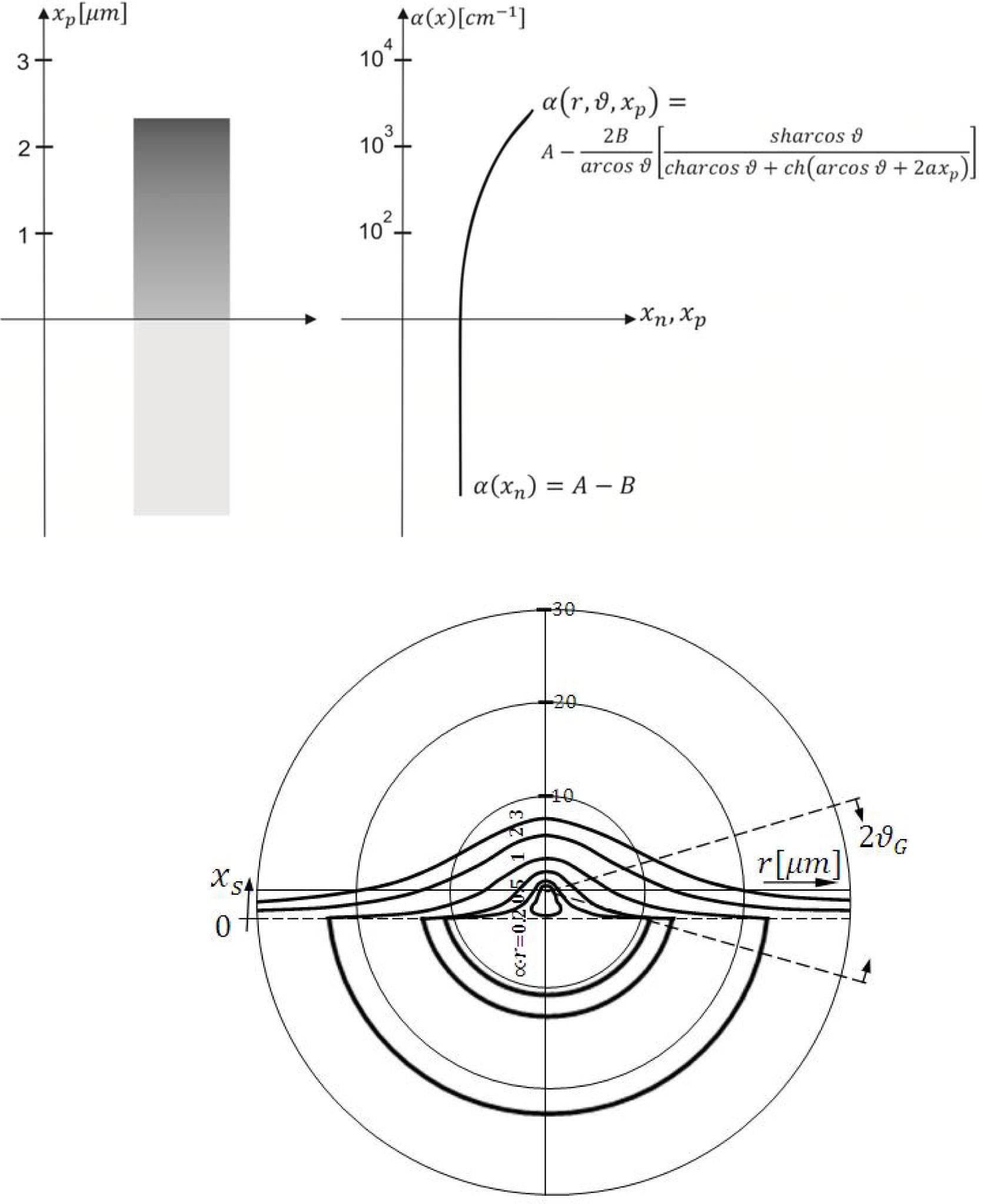
As an example, the intensity of the radiation field around a fixed point source at xp=3 µm is shown in Figure 3 in dependence on rs for different directions (Parameter values for absorption function α(x)=A – β · ch2ax; A=5.1 · 103cm-1, β=5 · 103cm-1, a=2 · 103cm-1). In the coordinate system formed by r and ϑ, lines of constant intensity are drawn, with r=|r→|=|r→s−r→p|, and ϑ is the angle between x-direction and r→. The field is rotationally symmetric relative to an axis through xp perpendicular to the y – z plane. The sketched cone with an aperture of 2ϑcorresponds to the interval between the limiting angles (nGaAS ≅ 3,6). All rays outside the cone are not allowed to escape from the sample owing to total reflection. In the cone of a homogeneous medium the lines of constant intensity are circles [19]. That applies to the lower half plane in Figure 3. Wile for xs>0 the intensity depends strongly on α.
Radiation field around a point source. Full line: curves of constant intensity. Distance of the emitter from the interface, xp=3µm, r-length of radius vector between the excitation point (xp,yp,zp) and the point of observation. ϑ – angle between x direction and r→, ϑG– limiting angle. Absorption function is due to Equation (11). The solid curves correspond to values α·r=0.2; 0.5; 1; 2; 3
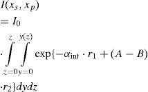
Now, we consider the intensity I(xs,xp)at the surface, given by the plane zs=0, if a layer of emitting points exists at the half plane x=xp, z<0. The intensity distribution of the emitting plane arises from a superposition of single intensity distributions given in Figure 3. The form of I(xs,xp) is
The connection line r between xs and each xp is divided into the partsr1 and r2(xs<0) by the interface at x=0. The upper bound y(z) of the inner integral is a function of the limiting angle ϑG=arc sin(n*)-1 as well as the emitter coordinates:
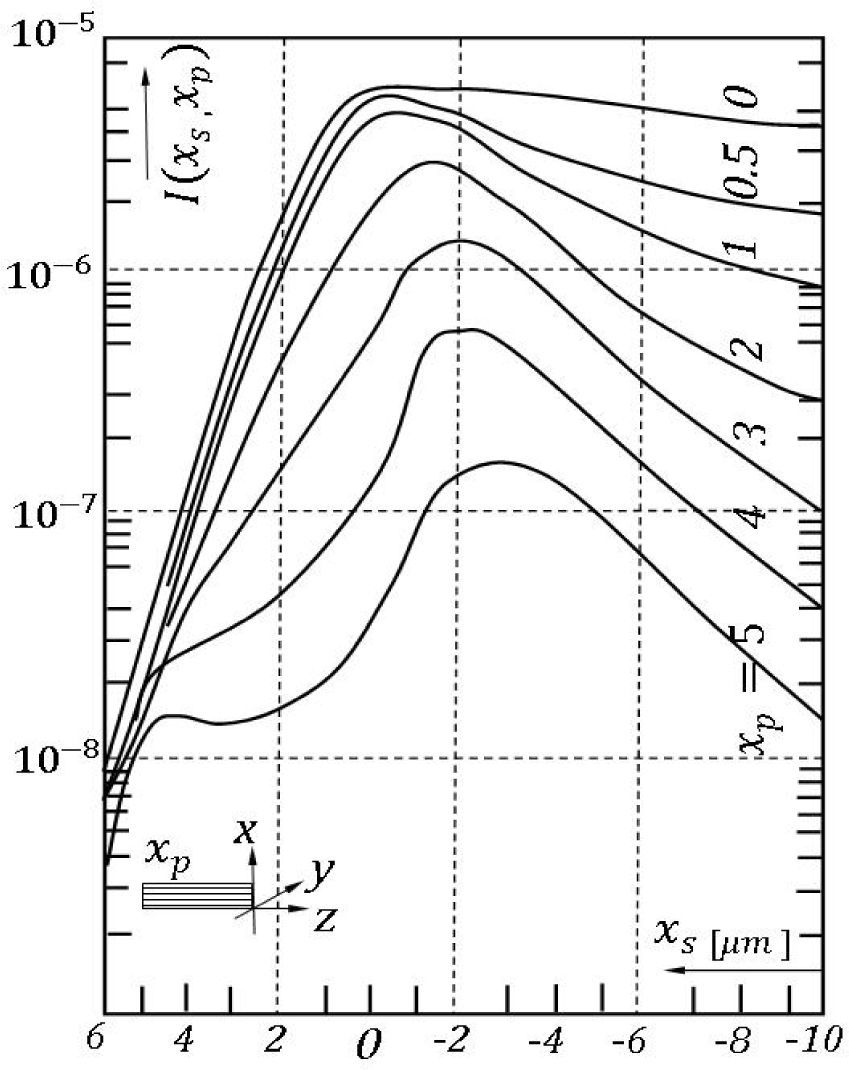
If we assume the same emission intensity for each of the emitters within a plane xp=const.,Equation 12 yields a run as shown in Figure 4. In this picture, curves are drawn for some emitter planes with different distances xp from the interface x=0. The intensity is given in dependence on the surface position coordinate xs.
It can be noticed that the maximum of the intensity I(xs,xp) of a layer at xp>0 is situated at xsm
This figure allows to construct the near field by simply superimpose the curves for different emitting layers xp, which prior to it have to be multiplied by a weight factor corresponding to the minority carrier density N(xp) at the recombination site, determining the intensity of the emission of involved layers.
Because of the much higher mobility μn of electrons relative to holes in GaAs (μn≈20μp) the recombination occurs within the p-region at places where the doping gradient is different from zero. The diffusion length L of electrons injected into the p-region is related to the concentration of acceptors, NA, as well.
5Time-dependent excitationAssuming that the minority carrier density N(xp, t) is known as a function of the co-ordinate xp and the time t, the construction of the near field under a.c.-condition is possible in the same way as it was suggested in the previous section.
In this case the total emitted radiation as well as the shape of intensity distribution will be changed during the time. For instance, if the current is switched-on at t=0, the layers are successively excited because of the finite diffusion velocity of the minority carriers into the region xp>0. At this, the maximum of intensity of the near-field moves downwards to negative xs– values, (i.e., into the opposite direction), because of the form of intensity curves in Figure 4. In order to obtain the near field for any time dependent injection the determination of N(xp,t) is necessary.
This spatial movement of the intensity maximum of the light field is the decisive property for the construction of an optical switch or a spatial routing of the outgoing optical signal.
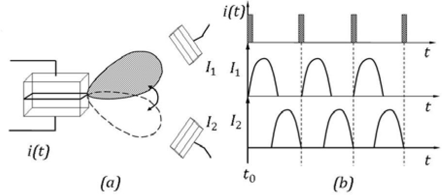
Let us consider the geometry as shown in Figure 5, where a LED illuminates a segmented photodetector. The segments are adjusted such that the light intensity maximum strikes each segment on its up and down turn corresponding to the time-dependent minority carrier injection.
(a) Light field of a LED under time-dependent minority carrier injection in front of a segmented photodetector. A current pulse injection i (t) and the response I1, I2 of segment 1 and segment 2, respectively, of the photodetector is shown in (b). Segments 1 and 2 of the photodetector register light signals, whose displacement in time depends on the minority carrier velocity in switching on and off the emitting layers, as described in Section 4.
Routing requires a relative displacement of the optical emitter signal with respect to the receiving elements. This is commonly done e.g., by switching a mirror between two positions. In the schematic arrangement here described, a property of the light field of spontaneously emitting Laser diode structures is applied, which represents itself by a slight up-and down movement of the maximum of the intensity band under time-dependent carrier injection. The treatment of light propagation inside the inhomogeneously absorbing bulk in a ray-like approximation has proved justified by previous experimental studies of the near and far field of LEDs. We find a displacement of the maximum intensity band on the side face of a Fabry-Perot cube in the order of 1μm between initiation and end of an excitation cycle. An even more pronounced and useful movement of the maximum intensity band is manifested in the far field pattern of the Fabry-Perot cube. The angular spread in space may reach up to 40°, as we had measured in an early work [20]. In the typical angular intensity distribution, the inclination ϑ of the maximum intensity direction I against the normal onto the light-emitting surface of the diode stretches over the interval 10°<ϑ<40° as a rule. This fact is presented in Figure 5(a).
A detector element of two segments with such geometrical dimensions is easy to construct and would produce, in a separated fashion, two outgoing signals, which additionally are spaced in time due to the diffusion velocity of the recombining excess minority carriers. It is interesting to consider this time spacing as a new experimental means to determine the drift velocity of minority carriers.
Furthermore, we should notice, that the intensity curves of Figure 3 are changed if we consider the diffraction effects connected with S1(r→) and higher terms of the series (3). The effects of these terms in the case of LEDs as treated here is not negligible because the condition |grad α|/k0α<<1 is not fulfilled satisfactorily. The diffraction into the region of strong absorption yields a further reduction of the light intensity especially for xp and xs greater than zero. Also the position and sharpness of the maximum intensity at z=0 for emitting layers at xp>0 may be influenced by this effect.


