


Because light emitting diodes (LEDs) have the advantages of dc working voltage, high luminescent efficiency, short ignition time, high reliability and pollution free, they have substituted for incandescent bulbs and fluorescent lamps gradually. In order to simplify circuit complexity, an active clamp forward converter with the sequential color display (SCD) control is proposed to drive red, green and blue (RGB) LED arrays. The proposed converter has zero-voltage switching (ZVS) operations of both the main switch and the auxiliary switch, resulting in high system efficiency. Driving RGB LED arrays sequentially by one converter can save components and reduce cost significantly. Additionally, the pulse-width modulation (PWM) control is applied to achieve a large chromaticity variation. The circuit operations are analyzed in detail and the circuit parameters are designed based on the practical considerations. Finally, an illustrative example is implemented to demonstrate the feasibility and validity of the proposed LED driver.
Recently, light emitting diodes (LEDs) have substituted for incandescent bulbs and fluorescent lamps gradually in the residential, industrial and commercial lighting applications [1], because they have the advantages of dc working voltage, high luminescent efficiency, short ignition time, high reliability and pollution free, etc. Moreover, since mixing multi-coloured LEDs can provide a large chromaticity variation, LEDs are progressively used in outdoor landscape lighting systems as well.
Figure 1 shows the block diagram of a photovoltaic powered landscape lighting system, in which an isolated DC/DC converter is used to fulfill a step-down conversion, govern the current through LED arrays and provide the electrical isolation of safety requirements. Generally, a colored LED module is composed of red, green and blue (RGB) LED arrays. Since RGB LEDs have different electrical characteristics, three isolated DC/DC converters are required to regulate the current through each LED arrays [2]. Therefore, the number of power components will become triple, resulting in large volume, high cost and low reliability.

In the literature [3, 4], a sequential color scanning scheme was proposed to reduce power consumption. LEDs are very suitable for a sequential color display (SCD) due to their fast response. When LEDs are displayed intermittently with high frequency, human cannot observe the darkness of short time intervals. The SCD control has been applied in a color LED backlight driving system for liquid crystal display (LCD) panels [5], [6], in which RGB LED arrays are sequentially driven by the same DC/DC converter.
Many isolated DC/DC converters for RGB LED driving, such as flyback and forward converters, have been presented in the literature [3, 5].However, their hard-switching operations reduce conversion efficiency and induce electromagnetic interference (EMI) noise. This paper proposes an active clamp forward converter [7-9] with SCD control as the color LED driver for a photovoltaic powered landscape lighting system. For this driver, due to saving transformers, power switches, control ICs and energy storage components, the circuit complexity can be simplified, and the system volume and cost can be significantly reduced. With accurate analysis and design, both of the main switch and the auxiliary switch can turn on under zero-voltage switching (ZVS), leading to higher system efficiency and lower EMI noise. Besides, the pulse-width modulation (PWM) control is applied to change the luminance of RGB LEDs so that a large chromaticity variation can be achieved. The operation principles are addressed. Experimental results of a 100W laboratory prototype are used to verify the feasibility and validity of the theoretical predictions.
2Operation principlesThe proposed color LED driver, as shown in Figure 2, consists of an active clamp forward converter and RGB LED arrays with SCD control. In this section, the operation principles of the SCD control and the proposed converter are introduced briefly in the following.
2.1Sequential color display control
To achieve SCD control, RGB LED arrays are connected in series with the switches SR, SG and SB, respectively. The switches are driven with phase-shift manner, as illustrated in Figure 3, in which vgs_r, vgs_gand vgs_bare their gate signals with the switching frequency fm. The frequency of the driving signals vGS1 and vGS2 in the active clamp forward converter is fs which should be much higher than fs. The voltages Vo_R, Vo_G and Vo_B are the forward voltage of RGB LED arrays, respectively. The currents iR, iG and iB are their corresponding driving currents.

Assuming that the currents iR, iG and iB have the same amplitude lP at full-load condition, the maximum average output-current lo,avg of a conventional RGB LED driver is 3lP. For the proposed driver, if the maximum duty cycle of the driving signals vGS_R, vGS_G and vGS_B are Dmax, then the maximum average output-current lo,avg is

Because Dmax is 33.33% in the proposed driver, lo,avg is only equal to lP. Therefore, the required output-power of the proposed driver is only one-third of that of a conventional driver, which results in energy saving significantly.
In the proposed system, the red, green and blue LED arrays are driven by the same converter sequentially, leading to small volume, low cost and high reliability. All of the driving signals vgs_r, vgs_gand vgs_bare produced by the digital signal processor (dsPIC30F4011). The luminance of each LED array is dimmable by modulating the duty of its driving signal, so as the color of the RGB-LED module is variable. The output capacitor C0 with low capacitance is used in the converter so that the output voltage can vary promptly according to the forward voltage of each LED array.
2.2Active clamp forward converterFigure 4 shows the circuit diagram of the active clamp forward converter. Each active switch S1 (S2) is composed of an MOSFET Q1 (Q2) and its intrinsic anti-parallel diode D1 (D2). The forward converter is formed by the main switch S1, transformer Tx, forward diode D3, freewheel diode D4, output inductor L0, and output capacitor Co. Instead of the reset winding in traditional forward converter, the auxiliary switch S2 and the clamping capacitor Cc are used to reset the residual flux of transformer. The residual energy of magnetizing inductor Lm can be restored to the input voltage source. Both of the main switch S1 and the auxiliary switch S2 can turn on under ZVS, resulting in low switching losses and high system efficiency.

For simplifying the analysis of operation principles, following conditions are made:
- 1)
All components are ideal.
- 2)
The capacitance ofCc is much higher than that of the intrinsic capacitorCds, and the inductance ofLm is much higher than that of the leakage inductorLr.
- 3)
Lo and Co are large enough so that the output voltageVo and output currentlo can be regarded as constant.
- 4)
The dead time between the driving signals ofS1 andS2 is very short and negligible. The turn-on intervals ofS1 andS2 are considering asDTS and (1-D)TS, in whichTs is the switching period in steady-state operation.
According to the volt-second balance concept, the relation of input voltage VB and the voltage across clamping capacitor vc can be expressed as

Arranging Eq. 2 yields

Eq. 3 indicates that vc is the output of boost-type operation with input voltage VB. When S1 turns off and S2 turns on, the voltage across main switch vds1 will be equal to vc and determined as

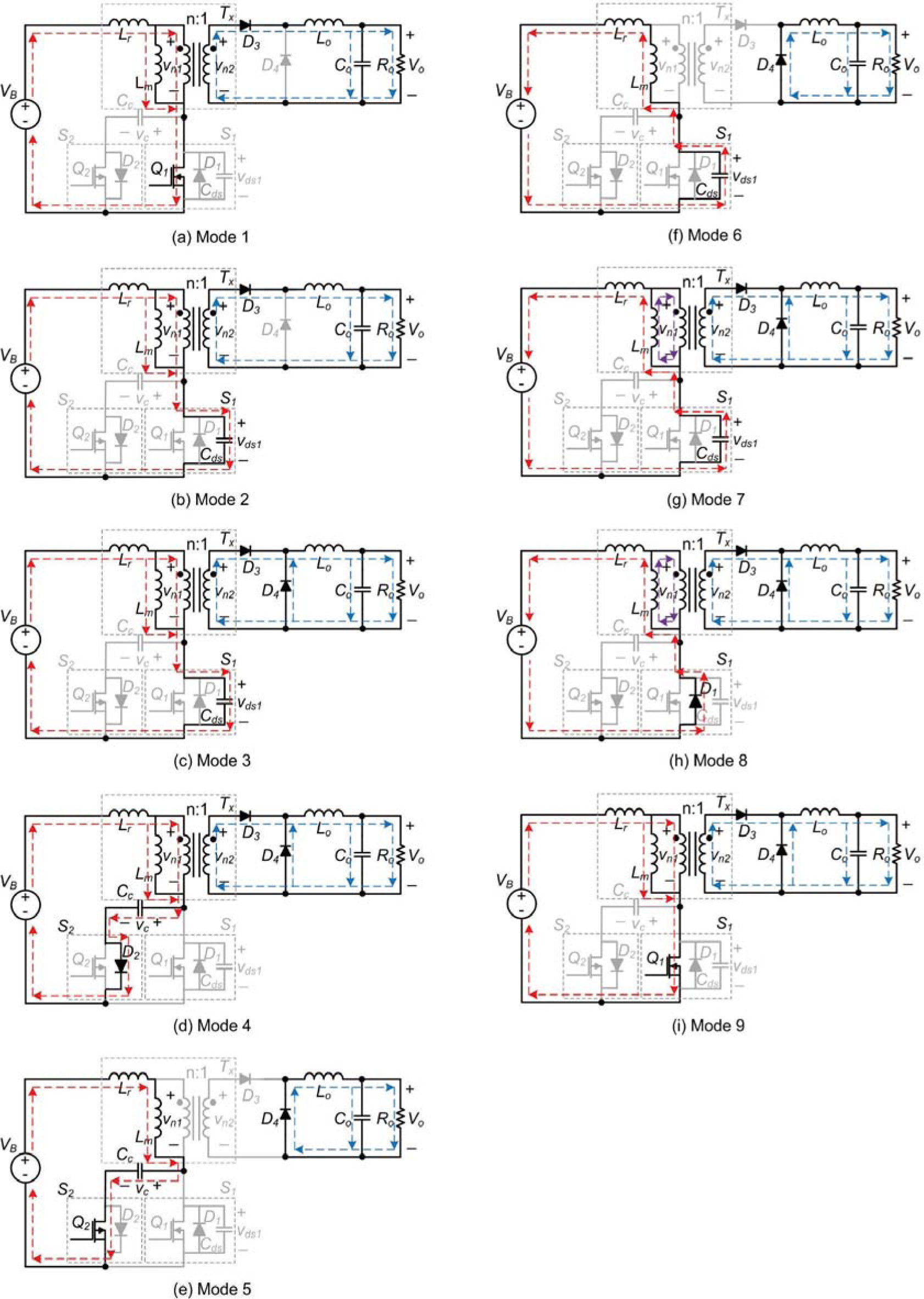
Figure 5 shows the theoretical waveforms of the active clamp forward converter, which is divided into nine operation modes within one switching period. The operation principle of each mode will be introduced referring to the equivalent circuits shown in Figure 6.


Mode 1 (t0~t1): At the moment t=t0, the switch S1 is turning on, and the switch S2 is turning off. Since the voltage across magnetizing inductor vn1 is equal to VB, its current iLm increases linearly. The voltage across secondary winding vn2 is VBI n so that the forward diode D3 turns on and the freewheel diode D4 turns off. The input voltage source charges output inductor Lo through the transformer Tx and D3. This mode ends while the gate signal of S1 disappears.
Mode 2 (t1~t2): At the moment t=t1, the main switch S1 turns off, and the current iLr charges the intrinsic capacitor Cds of main switch. The voltage vds1 increases, and the voltage vn1 decreases. This mode ends while vds1 reaches VB.
Mode 3 (t2~t3): At the moment t=t2, the voltage vn1 reaches zero so that D3 and D4 are both turn-on. Since the diode current iD3 decreases, the leakage inductor current ¡Lr decreases as well. The magnetizing inductor current iLm remains the same. This mode ends while vds1 reaches VBI (1-D).
Mode 4 (t3~t4): At the moment t=t3, the main switch S1 turns off. The current iLr flows through anti-paralleled diode D2 to transfer energy to the clamping capacitor Cc, which provides ZVS operation for the auxiliary switch S2 turn-on. Gate signal of S2 should be applied during this mode. This mode ends while iD3 reaches zero.
Mode 5 (t4~t5): At the moment t=t4, because the current iD3 is zero, the inductor Lm is in series with Lr and participates in the resonance with Cc. The voltage vn1 is DVBI (1-D) with reverse polarity. The resonant current iLr is equal to the current iLm and remains decreasing. While iLr becomes negative during this mode, the energy of Lm will be restored to the input voltage source. This mode ends while the gate signal of S2 disappears.
Mode 6 (t5~t6): At the moment t=t5, the auxiliary switch S2 turns off, and the resonant current iLr follows through the intrinsic capacitor Cds to discharge it. This mode ends while the voltage vds1 decreases to VB.
Mode 7 (t6~t7): At the moment t=t6, the voltage vds1 is equal to VB so that the voltage vn1 becomes zero again. Since D3 are turning on now, its current iD3 increases and the current iLr increases as well. The magnetizing inductor current iLm remains the same. This mode ends while vds1 reaches zero.
Mode 8 (t7~t8): At the moment t=t7, the current iLr-flows through anti-paralleled diode D1 to transfer energy back to the input voltage source, which provides ZVS operation for the main switch S1 turn-on. Gate signal of S1 should be applied during this mode. The current iLr increases from negative with the slope of VBI Lr. This mode ends while iLr- reaches zero.
Mode 9 (t8~t9): At the moment t=t8, the current iLr becomes positive. The current iD4 is decreasing continuously, and this mode ends when iD4 reaches zero. When the diode D4 is turned off at t=t9, the operation goes to Mode 1 of the next high-frequency switching cycle.
3Design proceduresBased on the operation principles presented previously, the proposed color LED driver with the specifications listed in Table 1 is taken as an illustrative example. The designed procedures of the active clamp forward converter are described as follows.
Step 1-Select fs and D: Select the switching frequency fs as 150 kHz. For the normal operation condition with 24 V battery voltage and full load output, the duty ratio D of the main switch S1 is determined as 0.5.
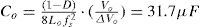
Step 2-Determine n: Considering that the forward voltage Vf of the diode D3 is around 0.7 V, the minimum turn ratio (n) of the transformer Tx can be determined as

In the illustrative case, (n) is set as 1.
Step 3-Determine Lo: In order to minimize the output ripple current and reduce the current stress of power components, we select 10% of maximum output current as the boundary condition. The boundary inductance of L0 can be obtained as
In the illustrative case, Lo is set at 100μH.
Step 4-Determine Co: While output inductance Lo is determined, considering that the specification of ΔV0 is 10mV, the capacitance of Co can be obtained
The standard capacitance with 33μF is selected for Co.
Step 5-Determine n1: Select core material as TDK PC40 and core size as EE-19. Its saturation flux density Bsat is 4500 G at 60 °C, and effective cross area Ae is 0.23cm2. To avoid core saturation, we set the maximum flux density Bmax at half of Bsat. Therefore, the turn number of primary winding n1 can be calculated as
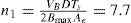
In the illustrative case, n1 is set as 8. The inductance of Lm can be measured as 80μ.
Step 6-Determine Lr: According to the operation principle of Mode 6, the current iLr at t=t6 can be obtained from following
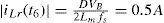
To achieve ZVS operation of the main switch S1, the inductance of Lr should meet following equation

Considering that the intrinsic capacitor Cds of IRF530 is 190 nF, the required inductance of Lr can be obtained as 438 nH.
Step 7-Determine Cc: To optimize the voltage stresses of Cc, S1 and S2, the period of the resonance occurring during S1 turning-off should be longer than ten times of the turn-off time of S1, which is expressed as

Thus, the minimum capacitance of Cc can be obtained as
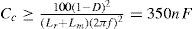
The standard capacitance with 470 nF is selected for Cc.
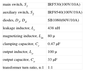
The calculated component parameters of the illustrative example are summarized in Table 2.
Component Parameters of the Prototype.
| main switch, S1 | IRF530(100V/10A) |
| auxiliary switch, S2 | IRF9540(100V/19A) |
| diodes, D3, D4 | SB1060(60V/10A) |
| leakage inductor, Lr | 438 nH |
| magnetizing inductor, Lm | 80μ |
| clamping capacitor, Cc | 0.47μF |
| output inductor, Lo | 100μ |
| output capacitor, Co | 33μF |
| transformer turn ratio, n:1 | 1:1 |
While input voltage VB is 24 V, Figure 7 shows the measured waveforms of the output voltage Vo and the output inductor current iLo at full load operation. It can be seen that Vo is regulated at 11.41 V, and the average output current is 2.04 A, which are very close to the required specifications. The measured waveform of clamping capacitor voltage Vc according the driving signal VGS1 is shown in Figure 8. It is obvious that resonance with the frequency determined by Cc and (Lr+Lm) occurs after the main switch S1 is turning off. In this time interval, the resonant current iLr transfers energy from Lm to Cc, and then restores energy to the input voltage source.
.")
.")
Figure 9 shows the measured voltage and current waveforms of the main switches S1 at full load condition. It could be observed that S1 can turn on under ZVS condition. Figure 10 shows the measured voltage waveforms of the auxiliary switches S2 at full load condition. The drain to source voltage vds2 becomes zero before the driving signal VGS2 is supplied, from which the ZVS operation of S2 can be verified. Therefore, the switching losses can be significantly minimized to improve system efficiency.
.")
.")
Figure 11 shows the measured efficiency curve of the proposed color LED driver with 24 V input voltage. The maximum efficiency is up to 92.5% at /0=1.6 A. The normal operating range for driving color LED arrays is from 1.2 A to 1.8 A. The system efficiency can be kept above 91% in this range, which provide energy saving significantly.

Figure 12 shows the measured waveforms of output voltage Vo and output current Io while the LED module outputs “white” light. It can be seen that red, green, and blue LED arrays are driving in sequential and with the frequency of 30 Hz. The output voltage Vo is around 10.4 V for driving red LEDs, and Vo is regulated to around 11.4 V for driving green and blue LEDs. The duty cycle of each LED is almost 100% so that all of them provide the highest luminance to have “white” light output. In Figure 13, the duty cycle of green LEDs is changed to be 50% to reduce the luminance. Since the luminance of red and blue LEDs remain 100%, the color of the light provided by LED modules is “purple”. These experimental results verified that a large chromaticity variation can be achieved by low-frequency PWM control. By the way, the photo of the illustrative prototype is shown in Figure 14.
.")
.")

An active clamp forward converter with the SCD control for driving RGB LED arrays has been proposed. ZVS turn-on operations of both the main switch and the auxiliary switch lead to low switching losses and high system conversion efficiency. RGB LED arrays are sequentially driven by the same converter, which can save components and reduce cost significantly. Besides, PWM control is applied to achieve a large chromaticity variation. Experimental results of a 100 W illustrative example have really proved the feasibility and validity of the theoretical predictions.
AcknowledgementsThis work was supported by the National Science Council of Taiwan, Republic of China, under grant contract NSC 101-2221-E-214-059.