


Commonly, organic electronics devices are build up from the organic semiconductor thin films which are prepared either by thermal vacuum evaporation or by solution-processing techniques such as spin casting, inkjet printing, or roll-to-roll printing. The solution-processing has several advantages although it has a crucial problem for multilayer device preparation where the first layer will be dissolved by the solvent of the second layer. The using of insoluble layer is a solution of this problem. This paper reports the electrical (I-V) characteristics of Hole-Only Devices (HOD) which are prepared via solution processing by using insoluble layer. The insoluble layer based on triphenylamine dimmer was sandwiched in the two electrodes as anode and cathode. This insoluble layer was prepared via oxetane ring-opening polymerisation either oxidative crosslinking, photo crosslinking, or trityl crosslinking. The measurement was carried out to get current density versus electric-field strength characteristic as a function of oxidation potential, polymerisation mechanism, the amount of oxidant, and curing temperature. The measurement confirmed that the crosslinked hole-transport layers are successfully applied in HOD, the oxidative crosslinking mechanism showed the doping effect, and the amount of oxidant influences the conductivity of crosslinked layer.
Organic electronics devices have been developing rapidly in the recent year. It based on organic semiconductor which are π- conjugated materials, either small molecules or polymer (Müller et al., 2003). They have energy gaps ranging from about 2 eV to 3,5 eV, and have essentially no free carries at room temperature.
Organic semiconductor thin films are prepared either by thermal vacuum evaporation or by solution-processing techniques such as spin casting, inkjet printing, or roll-to-roll printing (Yang et al., 2006; Müllen & Scherf, 2006). It is known also that the solution-processing offers the possibility for large-area and low-cost fabrication but it has a crucial problem for multilayer device preparation where the first layer will be dissolved by the solvent of the second layer. The solution of this problem has been developed through preparation of insoluble layer via cationic ring-opening polymerisation of oxetane-derivatized (Rudati et al., 2012; Müller et al., 2000; Reufer et al., 2005; Bacher et al., 2005), which is called crosslinking. Many experiments related with the application of insoluble layer via cationic ring-opening polymerisation (CROP) of oxetane-derivatized or crosslinking have been reported (Müller et al., 2003; Yang et al., 2006), but the investigation results of the electrical characteristics of single crosslinked hole-transport layer are not included.
This paper reports the effect of process parameters of cationic ring-opening polymerisation of oxetane-derivatized on hole-only devices (HOD) characteristics. The investigation has been carried out to investigate the influence of crosslinking mechanism and the variation of process parameters to the single insoluble hole-transport layer. The electrical characteristics of HOD due to the oxidation potential of oxetane-derivatized triphenylamine dimmer (XTPD) HTL materials, the various crosslinking mechanism, the various amount of doping, and the various crosslinking process parameter were investigated and discussed. This characteristics are presented as current-voltage (I-V) characteristics by j-E curves, where the current density (j) depends on the electric-field strength (E). Further more, the cationic ring-opening polymerisation of oxetane-derivatized mechanism is called crosslinking in this paper.
1.1The oxetane-derivatized triphenylamine dimmer (XTPD) materialsTPD is known as hole-transport materials. It is a p-type semiconductor (Ganzorig & Fujihira, 2000) and has a low energy barriers for hole injection from the anode (O’Brien et al., 1998). In multilayer organics LED prepared via vacuum evaporation, it is sandwiched between anode and emitter layer (Hadziioannou & Malliaras, 2007) to enhance the device efficiency. In this case, it is applied as an electronics stair between anode and emitter layer which has a deep HOMO level.
Oxetane, like the other cyclic ethers, can be polymerised cationically under ring-opening. After initiation, the activation of an oxetane ring by proton or cationic, the polymerisation follows via nucleophilic attack of an ether on the activated ether. There are several necessary properties of oxetane. It is being inert under the strongly base condition of transition-metal-catalysed coupling reaction. It shows also a low volume-shrinkage
The TPD, as hole-transport material combined with spacer and oxetane ring, is crosslinkable and gives the possibility to polymerize via cationic ring opening polymerisation (Bacher et al., 2005). According to the oxetane properties, the polymerisation thin film should show only little volume shrinkage, short conversion time, and nearly quantitative yield. In other case, polymer films have better mechanical integrity than films of small molecules because the polymer chain is held together by strong covalent bonds whereas there is only weak Van der Waals attraction between molecules in a molecular film (Müller et al., 2003).
The redox chemical properties of the cross-linked films were investigated by cyclic voltammetry or electrochemistry measurement. After cross-linking, the films are perfectly stable during cyclovoltammetry (Shirota et al., 1994). The oxidation potential which is resulted in electrochemistry measurement is thermodinamically quantity and not the absolute value. This value has to be converted in the eV energy scale which refers to the vacuum energy value (0 eV). Therefore it can be compared to the work function or the energy value of Ultraviolet Photoelectron Spectroscopy (UPS)
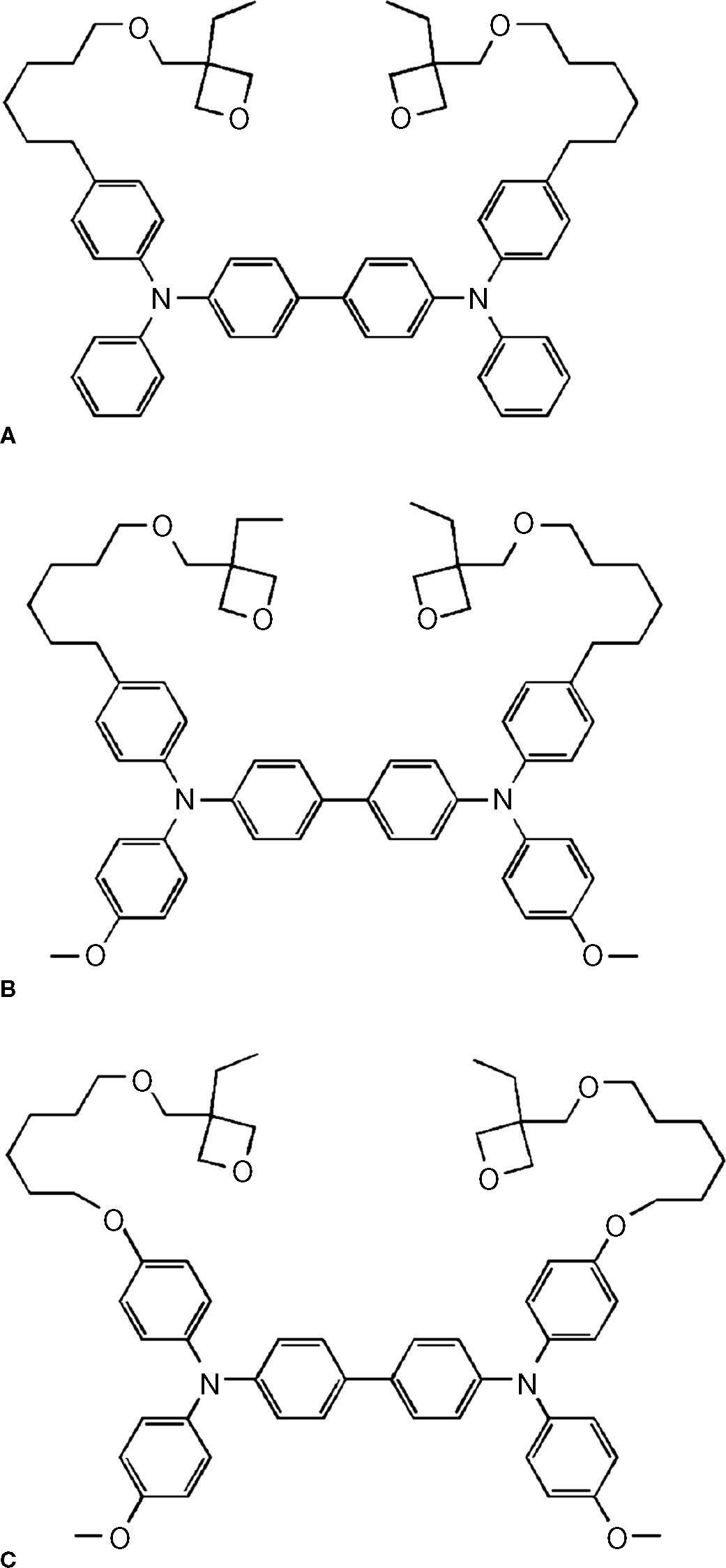
There are three kinds of XTPD HTL crosslinkable materials that were used in this experiment. They are called as XTPD1, XTPD2, and XTPD3 (Fig. 1), where the oxidation potential of XTPD1 is the highest, and the one of XTPD3 is the lowest. All of these materials are not commercially available.
1.2Cationic ring-opening polymerisation (CROP) of oxetane-derivatized
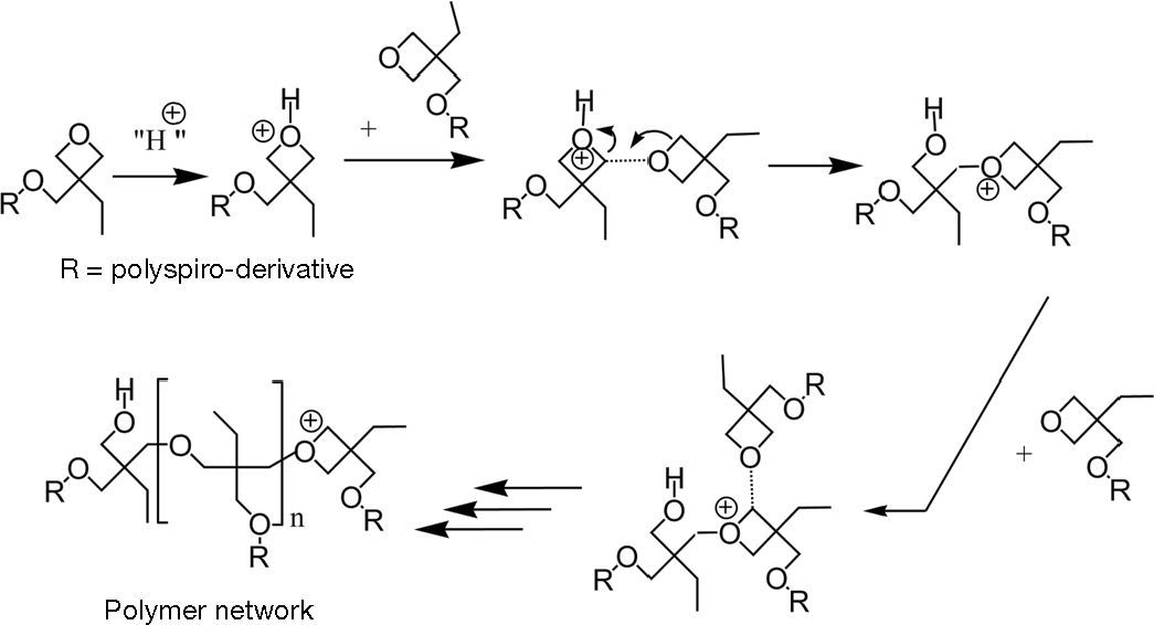
The CROP is the polymerisation mechanism which is started by opening the oxetane ring. Once an oxetane ring is opened, it will be continued by opening the next ring as shown in Figure 2 Generally the oxetane ring will be opened when it reacts with proton. This mechanism is utilised to polymerise a functional chemical group by attaching oxetane on it. In this investigation, a crosslinkable hole-transport material has been tailored by attaching oxetane on triphenylamine dimmer (TPD), and known as oxetane-drivatized triphenylamine dimmer (XTPD).

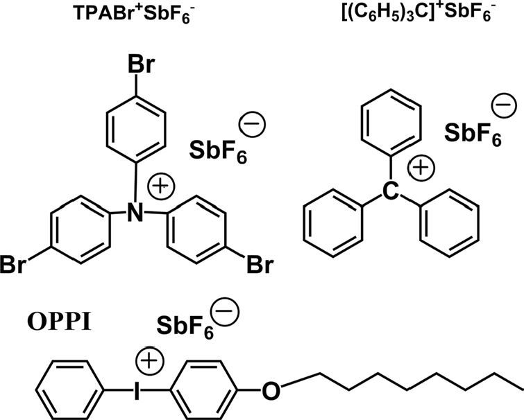
There are several mechanism to carry out CROP of oxetane-derivatized or crosslinking. In this investigation we focused on the three well known mechanisms. There are oxidative crosslinking, photo crosslinking, and trityl crosslinking which used tris(4- bromophenyl) aminium-hexafluoroantimonate (TPABrSbF6), 4- octyloxydiphenyliodonium hexafluoroantimonate (OPPI), and tritylium-hexafluoroantimonate ((C(C6H5)3SbF6) as oxidant, photo initiator, and trityl salt respectively. The chemical structure of this oxidant, photo initiator, and trityl salt are presented in Figure 3.

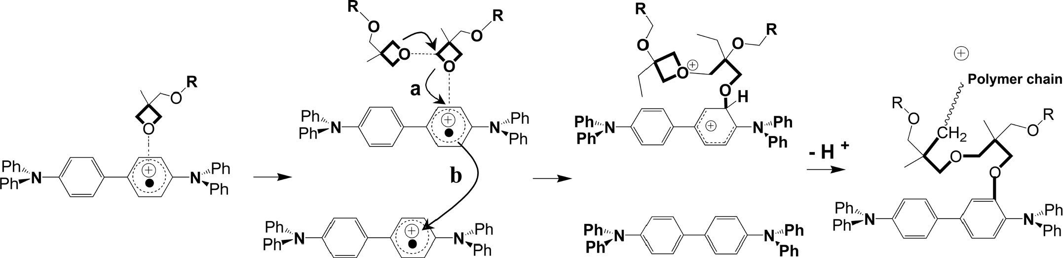
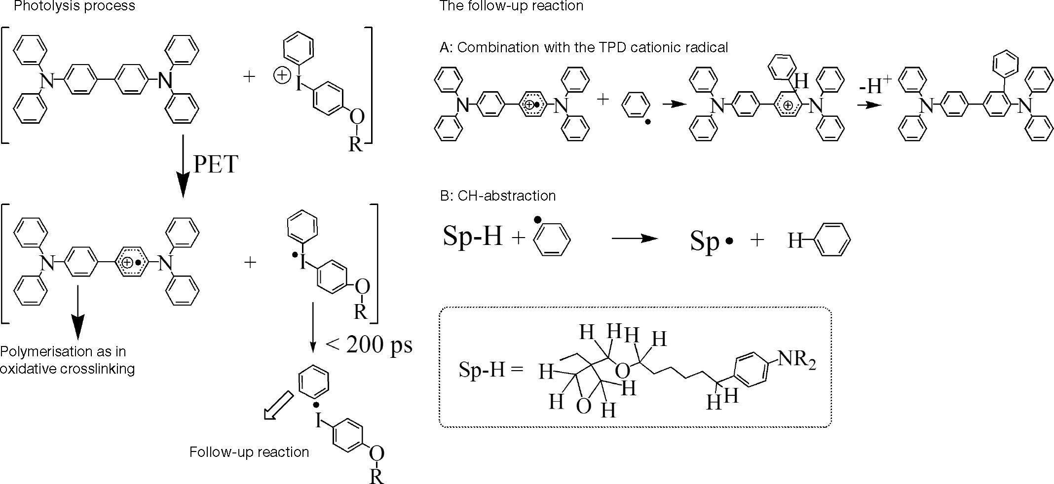
In the oxidative crosslinking, the oxetane ring is attacked by a TPD cationic radical (TPD+•). The TPD+• is produced in an oxidation reaction between a crosslinkable oxetane derivatized material and an oxidant. The oxidation reaction resulted TPD+• and at least two TPD+• is needed to open the oxetane ring (Fig. 4).

It is reported that the reaction between TPD+• and oxetane is possible in two ways. In the first possibility, the reaction is started by transfering the electron from the first TPD+• to the second TPD+•. This reaction results in TPD++ and TPD. The oxetane may attack the TPD++. In the second possibility, the oxetane attacks a TPD+• firstly and then the electron is transferred to the second TPD+• to find a stabile product. Therefore, this reaction does not include TPD++. The reactions above are followed by opening the oxetane ring. After that, a proton is abstracted and it can initiate another chain by acting as an electrophile.
It is reported (Rudati et al., 2012) that, in photo crosslinking mechanism (Fig. 5), the reaction is initiated by photolysis between XTPD and the iodonium (generally onium) photoinitator via irradiation with 365 nm UV-light. The reaction produces TPD+• and iodonium radicals. The iodonium radicals will decompose very fast and irreversibly by breaking of the C-I bond in phenyliodonium and phenyl radical (4). This phenyl radical may react with TPD+• in a follow- up reaction A and B.

In the follow-up reaction A, the generated proton can open oxetane ring of TPD+• to initiate the polymerisation. In the reaction B, the phenyl radical might react with alkyl spacer by H-abstraction (Rudati et al., 2012). The follow-up reaction B is non-desired reaction in the photo crosslinking, leading to uncontrolled radical reactions. The other reaction possibility is the reaction between oxetane and TPD+• as like in oxidative crosslinking.
In the trityl crosslinking mechanism, the polymerization is initiated via ring opening oxetane by trityl cation. In this case, trityl cation acts as electrophiles. Unlike in oxidative and photo crosslinking, there are no TPD cationic radicals (TPD+•) included in the polymerization reaction.
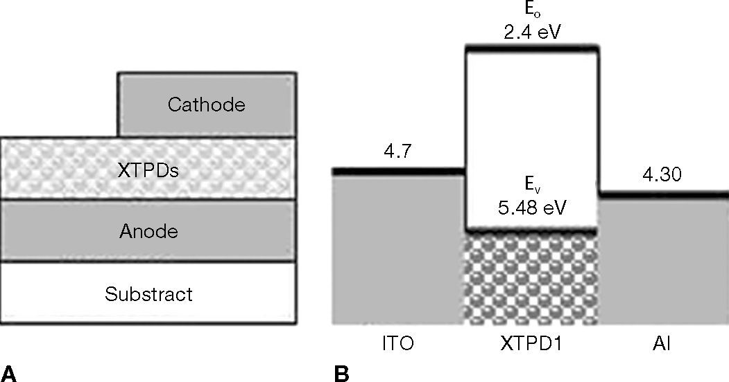
1.3Hole-Only Devices (HOD)The HOD is build up as a sandwich of crosslinkable hole-transport layer (XTPD) betwen two electrodes. The HOD used glass slices as substrate, indium tin oxide (ITO) as anode, and either aluminium (Al) or silver (Ag) as cathode. The hole-transport layer was prepared by spincoating and crosslinking. The cathode was deposited via thermal vacuum evaporation. Therefore, the structure of the HOD is ITO/crosslinked-HTL/cathode (Fig. 6A).

The fundamental process occurring in HOD is charge injection from the metal contact into the semiconductor film. This charge injection can be qualitatively understood by considering the electronic energy of the thin organic film (Fig. 6B). To inject electrons, the contact must be able to donate electron into the lowest unoccupied (LUMO) state, Ec. Similarly to inject holes, the contact must be able to accept electrons from the highest energy occupied state (HOMO), Ev. In the ideal Schottky model, the energy barrier to electron (hole) injection is:
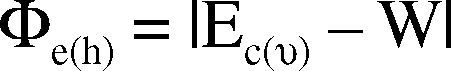
where W is the work function of the metal contacts.
According to the work function of ITO, Al and Ag, which are 4.7eV, 4.30eV and 4.60eV respectively, the major charge carrier is hole, because the barrier between LUMO level of XTPD and cathode is too high. The injected electron is negligible and the device acts as unipolar device.
2ExperimentIn this investigation the devices are prepared in several steps, which are substrates preparation, insoluble crosslinking film preparation, and cathode deposition. Firstly, ITO (indium tin oxide)-coated glass substrates were commercially obtained (20 Ω/in.2) and carefully cleaned and dried before use. After that, the ITO was treated by an ozone plasma.
The crosslinking layer of XTPD were prepared via three kinds of crosslinking mechanism which are known as oxidative crosslinking, photo crosslinking, and trityl crosslinking. In this experiment tris(4-bromophenyl) aminium-hexafluoroantimonate (TPABrSbF6), 4-octyloxydiphenyliodonium hexafluoroantimonate (OPPI), and tritylium-hexafluoroantimonate ((C(C6H5)3SbF6) were used as oxidant, photo initiator, and trityl salt respectively.
XTPD layer was prepared by spincoating a XTPD solution, which is added by a small portion oxidant or photo initiator or trityl salt on the ITO/glass substrate. The thin film thickness as 100 nm is controlled by spincoating duration and the angular velocity (rpm). The crosslinking of XTPD layers were carried out under 100 ¿C curing temperature for 1 minute, after irradiating with 365 nm UV light for 10 seconds. The films were rinsed with THF to remove the soluble decomposition products of the polymerisation, as well as non-cross-linked material. As cathode was 100 nm Al or Ag coated on the crosslinkable film via thermal vacuum evaporation to build up ITO/XTPD (100 nm)/cathode (100 nm) structure.
The investigation of I-V devices characteristics have been carried out for the various XTPD, the various crosslinking mechanism, the various amount of oxidant in oxidative crosslinking, the effect of process parameters as curing temperature and rinse treatment. The entire characterization was performed in a glovebox under inert gas atmosphere. This work was focused on the current-voltage characteristics of devices. Therefore, the node capacitance was not discussed.
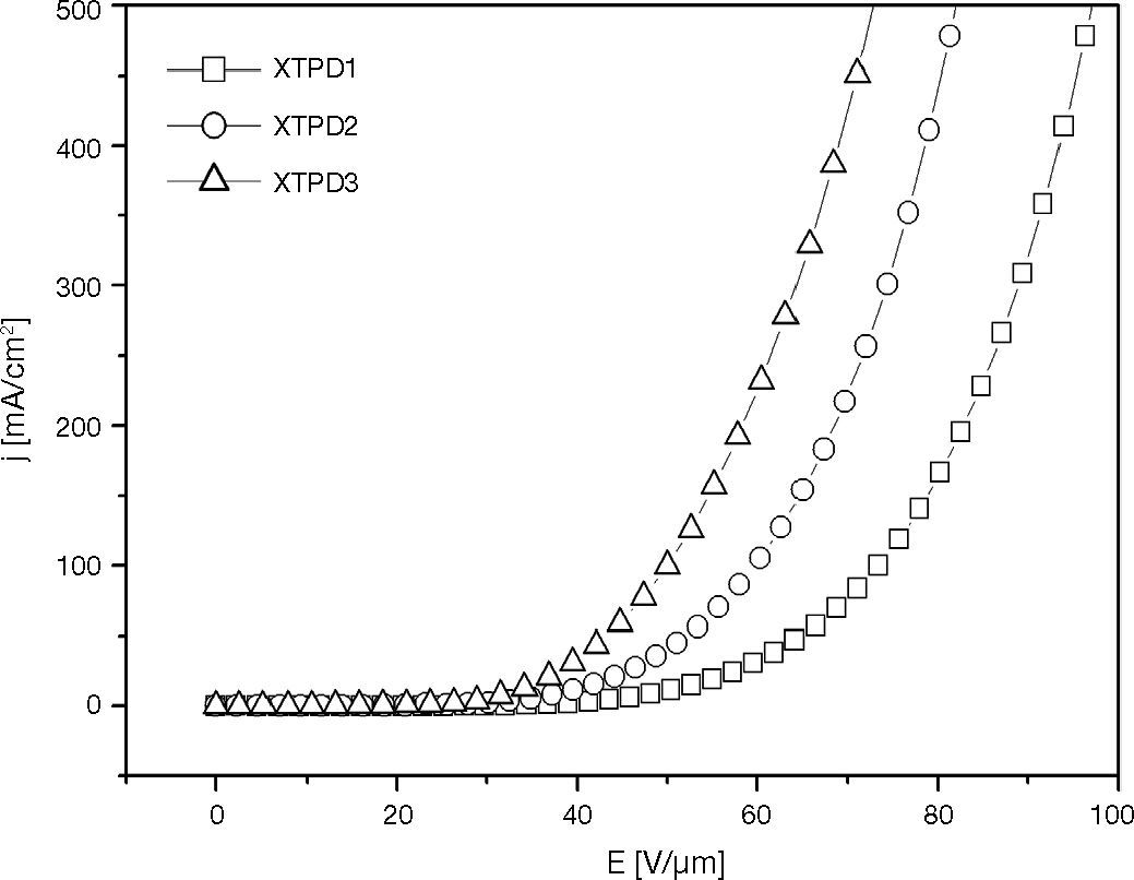
3Results and disscusion3.1The effect of XTPD oxidation potential on HOD characteristicThis investigation has been carried out for three kinds HOD. There are HOD1, HOD2, HOD3, which are based on XTPD1, XTPD2, and XTPD3 respectively. The XTPD crosslinked layer were prepared via oxidative crosslinking to build up the devices with ITO/XTPDS (100 nm)/Ag (100 nm) structure where the work function of ITO and Ag are 4,7 eV and 4,6 eV respectively.
The measurement results in Figure 7 show the j-E characteristics of HOD. The threshold voltage of HOD increase from HOD based on XTPD3 to the one based on XTPD1. The HOD with XTPD1 needs the highest operating voltage to achieve the same current density which is achieved by the other HOD.

Referring to the device structure in Figure 1, there is an electronic contact between ITO anode and XTPD layer in HOD. This contact creates hole-injection barrier (Φ) which is defined as the difference between work function of ITO and HOMO (Highest Occupied Molecular Orbitals) level of XTPD.
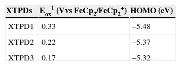
The HOMO level of XTPD is determined from its oxidation potential which is measured via electrochemistry with FeCp2/FeCp2+ as reference electrode. How deep the HOMO level relative to vacuum level is calculated as:

where 5,15eV is state as potential energy of FeCp2/FeCp2+. The determined XTPD oxidation potential and HOMO levels are showed in Table 1.
Remembering that work function of ITO is –4.7 eV relative to the vacuum level, the hole-injection barrier can be calculated as:
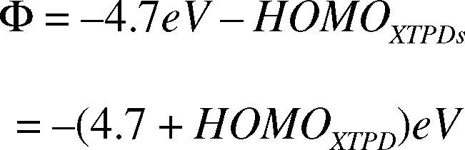
This equation shows that the hole-injection barrier increases with oxidation potential.
The investigation above shows a correlation between oxidation potential of XTPD and threshold voltage of HOD. The threshold voltage increases with the higher of oxidation potential. This phenomenon gives a possibility to adjust the threshold voltage by adjusting the oxidation potential of materials which is conducted by a chemical synthesis of materials.
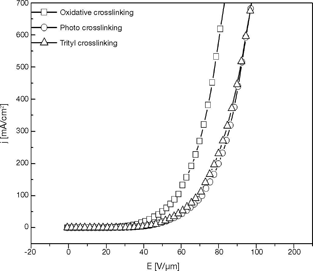
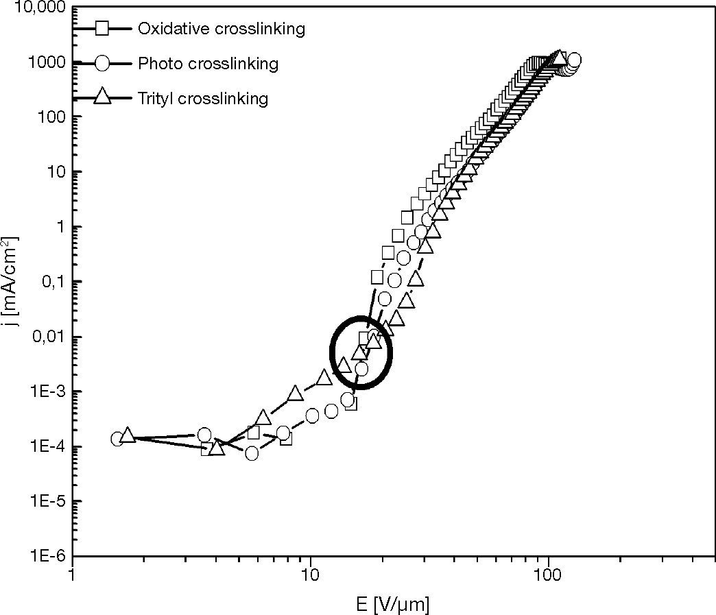
3.2Hole-only device with various crosslinking mechanisms layerInvestigating the relation between crosslinking mechanism and electrical characteristic of HOD was carried out by preparing the XTPD1 crosslinked layer via various crosslinking mechanisms. They are oxidative crosslinking, photo crosslinking and trityl crosslinking with 1,7% mole of oxidant, initiator, and trityl salt.
The characteristic curves in Figures 8 and 9 show that the threshold voltage of HOD are relatively same at about 20 V/μm, but at the voltage higher than threshold voltage the current density of oxidative-crosslinked HOD is higher than the other croslinked HODs. This phenomenon presents that the electronics barrier between ITO anode and HTL of those HODs were similar.
, photo-crosslinked HOD (), and cationic-crosslinked HOD ().")
, photo-crosslinked HOD (), and cationic-crosslinked HOD () in logarithmic scale.")
The difference of current density at a voltage higher than threshold voltage was caused by the difference of conductivity due to the charge carrier density in HTL.
The relationship between conductivity and charge carrier density can be presented as:
where σ is the conductivity, μ is the charge carrier mobility, and n is the charge carrier density.
According to the oxidative crosslinking mechanism (Rudati et al., 2012), the crosllinking is started by two TPD cationic radicals (TPD+•) that remain in the layer and act as charge carrier. In the photo crosslinking mechanism, the TPD+• which is included in reaction is less than in the oxidative crosslinking, and there is no TPD+• included in the trityl crosslinking mechanism.
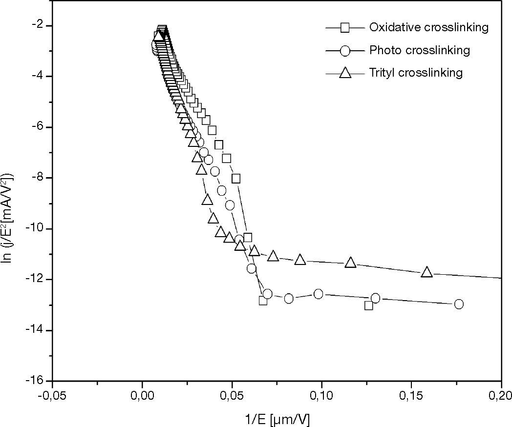
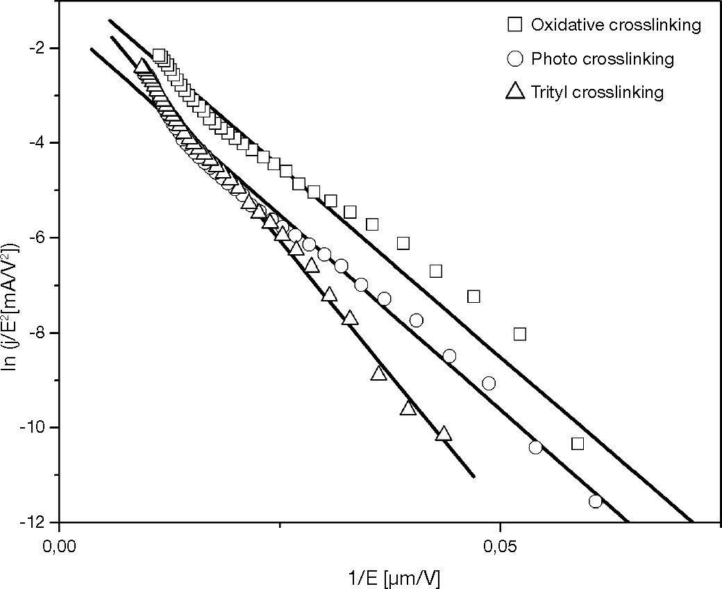
The approximation from Fowler-Nordheim equation is showed in the plot of ln(j/E2) vs 1/E in Figure 10. This plot is used to investigate the barrier height at the ITO/OTPD by Fowler-Nordheim tunneling predicts(5)
 vs1/E) for three kinds HODs.")
where j is the current density, F is the electric field strength, and is parameter which depends on the barrier shape. As predicted, the plot is closed to linear, particularly above the operating voltage. Deviation from linear at lower field strength is likely to be due to a thermionic emission contribution to the current.
By assuming that the injected charge is tunneling through a triangular barrier at ITO/OTPD interface, the constant is given by:(6)
Here is the barrier height and m* is the effective mass of the holes in XTPD. The electric field is assumed constant across the device.
The fitting curves of TPABrSbF6-HOD, OPPI-HOD, and trityl-HOD in Figure 11 show the similar slope for TPABrSbF6-HOD, and OPPI-HOD. The trityl-HOD has a slight difference slope than the other. According that α is obtained from the natural constant, the similarity of these slope indicates a constant barrier height for all the devices. The calculated barrier heights for hole tunneling into devices determined the barrier heights as 0.11 ± 0.02 eV.

Therefore, the crosslinking mechanism does not change the HOMO level of HTL nor anode-HTL barrier height. This mechanism changes only the crosslinked-HTL conductivity which depends on the charge carrier density (TPD+•) in HTL.
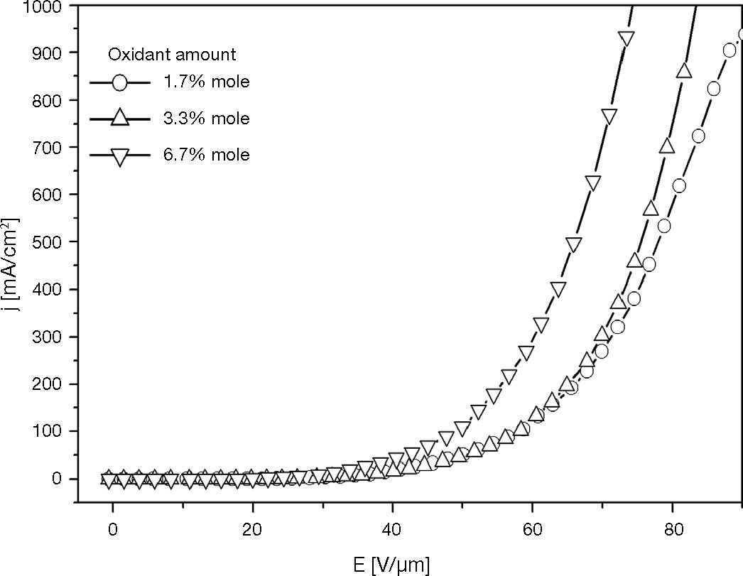
3.3The effect of various amounts of oxidant on HODAccording to the crosslinking mechanism (Rudati et al., 2012), there is a correlation between the amount of oxidant and the amount of cationic radicals (TPD+•). The oxidative crosslinking creates TPD+• in crosslinked films, and its amount increases with the oxidant amount. The effect of cationic radicals (TPD+•) to HOD characteristic was investigated by using variation of the amount of oxidant in oxidative crosslinking.
The curves in Figure 12 show the j-E characteristic of HODs which are prepared via oxidative crosslinking of XTPD1 with 1.7% mole, 6.7% mole, 13.3% mole of oxidants. The current density at high electric-field (above 40 V/μm) increased with oxidant amount, and the current density was highest in the HOD with the highest amount of oxidant.

Therefore, the j-E slope of HOD with 6,7% mole is higher than those of the others HOD. It indicates that the conductivity of films is increased by the existence of TPD+• in hole-transport layer. These results demonstrate that TPD+• in hole transport layer acts as doping species which changes the conductivity.
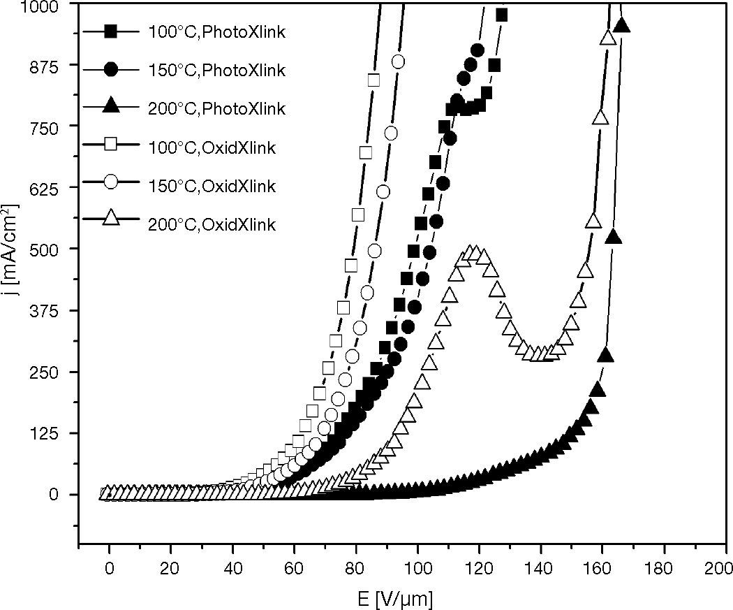
3.4The effect of curing temperature and rinse treatment on HOD characteristicIn curing-temperature experiment, hole-transport layers were prepared via oxidative crosslinking, and photo crosslinking of XTPD1 with 3.3% mole TPABrSbF6, OPPI repectively. The layers were irradiated with 365 nm UV light for 10 seconds and curing with variation curing temperature 100 °C, 150 °C, and 200 °C for 1 minute. These films were rinsed with THF before Al as cathode was deposited on it.
The results in Figure 13 show that the current density was decreased by increasing curing temperature and also by rinse treatment. As consequence, the HOD with higher curing temperature needed the higher operating voltage to achieve the same current density with the other HODs.

According to the crosslinking mechanism, the oxidation crosslinking film consists of much more TPD+• than photocrosslinking film. At curing temperature 200 ¿C, many of TPD+• was burned out therefore the conductivity was decreased and caused the deterioration on oxidation crosslinking film. This effect was not found on the photocrosslinking film which has not much TPD+• as on the oxidation crosslinking film.
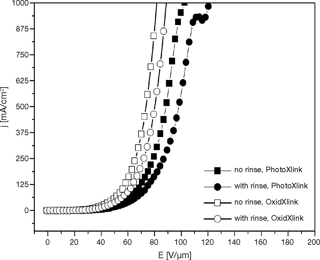
In rinse treatment experiment, two similar series of hole-transport layers were prepared via oxidative, and photo croslinking if XTPD1 with 3.3% mole TPABrSbF6, OPPI respectively. Films were crosslinked with standard procedure. After that, one series of samples was rinsed with THF and the other similar series was not rinsed before 100 nm Al was deposited as cathode.
The curves in Figure 14 show that the rinsed-series HOD needed higher operating voltage than those of no-rinsed-series HOD to achieve the same current density. The conductivity of layer decreases with rinse treatment, because during this treatment the small molecule species like uncrosslink XTPDs as well as it's cationic radicals leave the substrates. After rinse treatment, only the crosslinked material remains on the substrate.

Therefore, application of curing and rinse treatment in crosslinked hole-transport layer will decrease the conductivity. The decreasing of conductivity in this experiment have a strong correlation with the decreasing of TPD+• amount in the hole-transport layer.
4The potential applicationsThis technology gives the possibility for preparing a multilayer device via solution process. The crosslinking mechanism does not change the HOMO level of hole-transport materials. Remembering that the HOMO level of materials can be adjusted via chemical synthesis, it can be applied as an electronics stair for hole charge carrier in multilayer device, i.e. blue-emitted OLED with deep barrier between anode and the blue-emmiter layer. The application in the multilayer blue emitted OLED improves the efficiency (Müller et al., 2000).
The investigation showed the doping effect in the oxidative crosslinked layer. Therefore, it offers also the possibility to adjust the conductivity of the hole-transport layer via oxidative crosslinking mechanism.
Exceptly the cathode metalisasion via vacuum thermal evaporation, temperature process of this technology is about 100 ¿C. Therefore the overall energy requirements is relatively low compare to the fully vacuum evaporation technology.
There is also the possibility to build up a particular diode via solution-processing. For special purpose, an oxetane can be attached to a functional chemical group to get a certain crosslinkable material. Therefore it is possible to build up a photochromic diode with special application for example as electronic switches, or electronic write and readout memory.
On the other side, this technology gives the possibility for the low cost fabrication according to the film preparation via solution process (spin-coating) compare to other technologies, like vacuum evaporation, which is more complicated (Rodriguez et al., 2011; Rendon et al., 2012). The solution process offer also a possiblity for large area fabrication as like roll-to-roll printing, where the area in the vacuum-evaporator technology is bondered by the large of vacuum chamber.
5ConclusionsThe investigation of I-V characteristics of single layer insoluble hole-transport layer based on TPD in the HODs has been carried out and discussed. Commonly, the crosslinked hole-transport layers are possible to apply in HOD.
The results showed that the crosslinking mechanism does not change the HOMO level of hole-transport materials. Therefore it gives the possibility to adjust the threshold voltage of devices by adjusting the HOMO level of hole-transport material which can be carried out via chemical synthesis.
Related to the conductivity of the device, the oxidative crosslinking mechanism offers the possibility of charge carrier doping. Doping effect is shown on the HOD based on oxidative crosslinked HTL. The conductivity increases with the amount of oxidant which is correlated with the amount of charge carrier.
The rinse treatment and the curing temperature has an influence to the conductivity of crosslinked HTL. The higher curing temperature and rinse treatment decreases the conductivity of HTL. This treatment correlated with the remain of TPD cationic radical as charge carrier in the layer.
This project was supported by the German Ministry for Science and Education (BMBF; HOBBIT and NAPOLI projects).
I would like to thank Dr. Ronald Alle for oxidation potential measurement and discussion. Also Philipp Zacharias and Burhan Yildiz for the preparation of the crosslinkable materials.