Continuous growth in the use of multimedia applications on portable devices makes the mobile computer systems have an increasing complexity. The functionalities of the used SOC chips and silicon intelligent properties in these portable devices are become complicated and hard to design. Traditional digital circuit designs adopt register transfer level with timing control methodologies, which focus on the datapath composition, timing control of registers, and the functions of combinational circuits. However, the huge amount of control and synchronous signals of the above components are difficult to design and debug. The timing costs of design and verification are increased dramatically. This paper proposed a new design methodology of digital system, called data-oriented methodology, to deal with the above problems, by using Bluespec SystemVerilog HDL and the corresponding tools. Instead of conventional timing-control mechanism, the data-oriented methodology adopts simple handshaking protocol, blocking transferring, and explicitly register/FIFO declaration for communicating between adjacent modules. The designs of FDCT/IDCT and pipelined MIPS-like CPU are adopted to compare the design costs of conventional timing-control and data-oriented methodologies. The chip performance and FPGA proven of these two designs are discussed
As the exponential growth of semiconductor technology make more transistors integrate in the chip. The increasing multimedia applications on portable devices also make the mobile computer systems have an increasing complexity. The functionalities of the adopted SOC chip and silicon intelligent properties are become complicated and hard to design. Meanwhile, the continuously growing of semiconductor technology makes the novel digital systems consist of huge amount of transistors. Accordingly, several novel design strategies, such as high-level synthesis [1] and electronic system level design are proposed to bridge the gap between system model and behavior synthesis. New hardware description languages, such as SystemC, SystemVerilog, and Bluespec SystemVerilog [2], are proposed to achieve the above goal. But these languages still lack a suitable design methodology to fulfill the requirements of rapidly modeling, synthesis, and implementation.
Conventional timing-control methodology [3] focuses on the synchronizing the registers in a digital system, controlling the enable/select signals, and guaranteeing the manipulated data can be stored at correct time. However, the central control of huge amount of synchronous signals and states is difficult to maintain and design, the debugging and verification period is extended accordingly.
This paper proposed a novel deign methodology, called data-oriented methodology, to overcome the above challenges, by using Bluespec SystemVerilog and the corresponding tools. Instead of centralized timing-control strategy, this methodology divides the whole complex datapath into several individual blocks. The simple handshaking mechanism and blocking mechanism are adopted to make sure the correctness of adjacent blocks, by monitoring the flow of the manipulated data, from ancestor blocks to the descendant blocks. Therefore the complex centralized control unit can be reduced as several simple distributed control blocks between two adjacent blocks. The designs of FDCT/IDCT and pipelined MIPS-like CPU are adopted to compare the design costs of conventional timing-control and data-oriented methodologies. The chip performance and FPGA proven of these two designs are discussed.
The rest of this paper is organized as following. Section 2 discusses some related works and literatures of electronic system level design and high level synthesis. Section 3 describes the data-oriented design methodology. Section 4 proposed the two examples, FDCT/IDCT and pipelined MIPS-like CPU, to demonstrate the proposed data-oriented design methodology. Section 5 compares performance and implementation effort of chip fabrication between conventional and proposed methodologies. Finally, the conclusion is drawn in Section 6.
2Related Works2.1Electronic System Level Design MethodologyThe continuously growing complexity of electronic systems [8][9][10]make the modern chip designs reach the size that can not be handled by conventional register-transfer level modeling and timing-control based design methodology. Therefore a new design approach, System-Level Design (SLD) [12] or Electronic System Level (ESL) [13] has been proposed to overcome this problem. The design of complicated wires and signals’ transfers are replaced by higher level representation, Transaction Level Modeling (TLM)[13], to improve the abstraction level of chip design and shorten the design cycle. An ESL modeling language, SystemC [20], is widely adopted to write abstracted behavioral-level module designs and TLM models. Since SystemC is a class of C++, the integrating of SystemC modules and conventional C/C++functions is easier than other hardware description languages, such as Verilog, VHDL, and SystemVerilog. The ESL modeling tools, such as CoWare Platform Architect and Carbon SOC Designer, can provide a whole system components, include processor models, bus models, peripheral model, DSP models, and other model templates, for rapidly composing a SOC system. The software testbenchs can be easily integrated into the above system for early hardware/software co-simulation.
The major advantages SystemC modeling comes from its actor-oriented approach [18], which separates behavior from communication by actor and channel, respectively. The complex timing and data dependences of detailed RTL hardware states and signals can be hidden. However, there still exists a high gap between ESL models and corresponding RTL designs. The SystemC models in an ESL system are designed for hardware/software co-simulation and co-verification. The abstraction models are hard to translate into RTL designs directly. The requirements of manually re-write RTL designs dramatically limit the population of SLD/ESL design methodologies and tools.
2.2High-Level SynthesisIn order to overcome the design complexity of system-level design, the High Level Synthesis (HLS) [14] is proposed. The HLS mechanism is a process of mapping the specifications of behavioral hardware description languages (HDL) into the corresponding register-transfer level (RTL) models and processing the following translation stages of conventional cell-based IC design flow, such as logic synthesis and physical synthesis. The generated RTL design is optimized and met the constraints of area and delay. Accordingly, the quality of the final result of the generated design depends on the translation algorithm of the HLS mechanism. If the RTL design generated by HLS is inefficient and dirty, the successive optimizing stages of the cell-based design flow can not help to turn. Therein the produced chip can not meet the timing and area constraints.
Most of the HLS algorithms [14], such as scheduling, allocation, and resource sharing algorithms, adopt number of state in the generated finite-state machine (FSM) and datapath area as the evaluating metrics. Some other works adopt control and data flow graph (CDFG) [15][16][17] to represents the hardware costs of the generated RTL design. However, these costs and evaluated metrics ignore important aspects of control datapath and accuracy of timing for control logics. The correct synchronizing timing and corresponding RTL circuits cannot be predicted in the behavioral-level design. The quality of the produced RTL design can not met the timing and area constraints of the target design. Therefore, most of the quality of the RTL designs generated by the behavioral-level models and HLS software can not be accepted by the customers and ASIC chip designers.
2.3The Integration of Electronic System Level and High-Level SynthesisDue to the increasing chip capacities and computation capabilities, the implementation of a chip has to fulfill the above requirements and keep all of the costs small. Electronic System Level (ESL) design methodology is proposed to overcome the above design challenges and reduce the time-to-market of a new SOC chip. The widely adopted ESL modeling language, SystemC, help to reduce the design cycle of creating a new ESL model. According to the above discussion, the platform-based ESL modeling tools, such as CoWare Platform Architect and Carbon SOC Designed, can rapidly provide a common SOC platform for reference but lacks a directly translation approach, from SystemC to RTL Verilog/VHDL. These ESL SystemC models and virtual platforms focus on either simulation speed or accuracy, but not both. It widely limits the reality and performance of adopting ESL flows. Although several commercial SystemC-based behavioral synthesis (a.k.a. high-level synthesis) tools, such as Cynthesizer by Forte Design Systems [19], CatapultC by Mentor Graphics [21], and NEC’s CyberWorkBench [22], is proposed to translate the SystemC models into RTL Verilog designs, the tools for efficiently map the SystemC models into acceptable RTL Verilog designs are still missing.
Adopting high-level synthesis (HLS) mechanisms from SystemC models to RTL Verilog/VHDL designs can offer possible solutions for bridging ESL models and chip implementations. Unfortunately, there are serious problems of architectural mapping from the SystemC mode. The quality of the derived RTL Verilog design is poor. That is because the HLS translating tools can not understand the good software algorithms in the SystemC model, and select a most suitable corresponding hardware design. The generated hardware design can not meet the requirements of area, speed, and power constraints. Most of the internal heuristics in the HLS tools are just some kinds of syntax and primitive mapping, but not algorithms recognitions and selections. Although some HLS tools adopts CDFG to understand the basic building blocks of the input software SystemC models, the exponential combinations of hardware configurations and datapaths make the HLS tools hard to decide. Accordingly, a new ESL design methodology and a new ESL language for both modeling and synthesis are very important for modern SLD/ESL design requirement. Therefore, in this paper, a novel design methodology, data-oriented design methodology (DODM), is proposed, by adopting a new ESL language, Bluespec SystemVerilog (BSV). The detailed discussion of DODM and BSV are listed in the following sections.
3Data-Oriented Design MethodologyConventional hardware designs are implemented by timing-control methodology. The functionality of this methodology is controlled by correct signal arrival time, and then fetch/store manipulated data [3]. If the digital system becomes complicated, this timing-control model is too hard to implement. Accordingly, the design space, algorithm implementation, and debugging facility are also limited. If the timing of the synchronous signal in the ancestor stage is varied, the completed time of this stage will be changed, the then the descendant stage will retrieval incorrect data at the expected time. Finally the overall operating results of this digital system are incorrect. Therefore a novel methodology, data-oriented methodology, is proposed to solve this problem. This methodology focuses on manipulating data and the dependence of source operands that generate the results, instead of controlling precise timing and signals. The result of current stage is the source data of the next stage. Therefore the detailed plan of conventional datapath that consist of control signals, multiplexor, and dedicated functional units can be replace by the data manipulating mechanism, called “rule”, and the simple handshaking mechanism, called “interface method”. Since the main consideration is the states of data, instead of datapath timing, the difficulties of complex chip design can be reduced by approaching the nature of algorithm and shorten the design cycle.
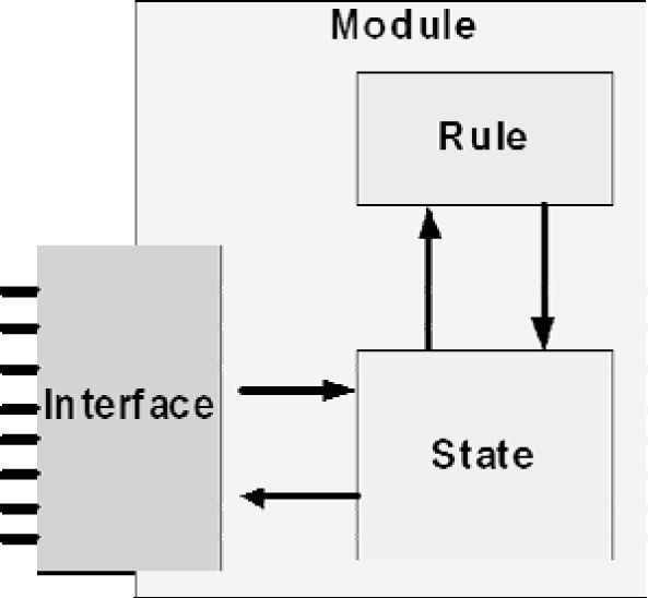
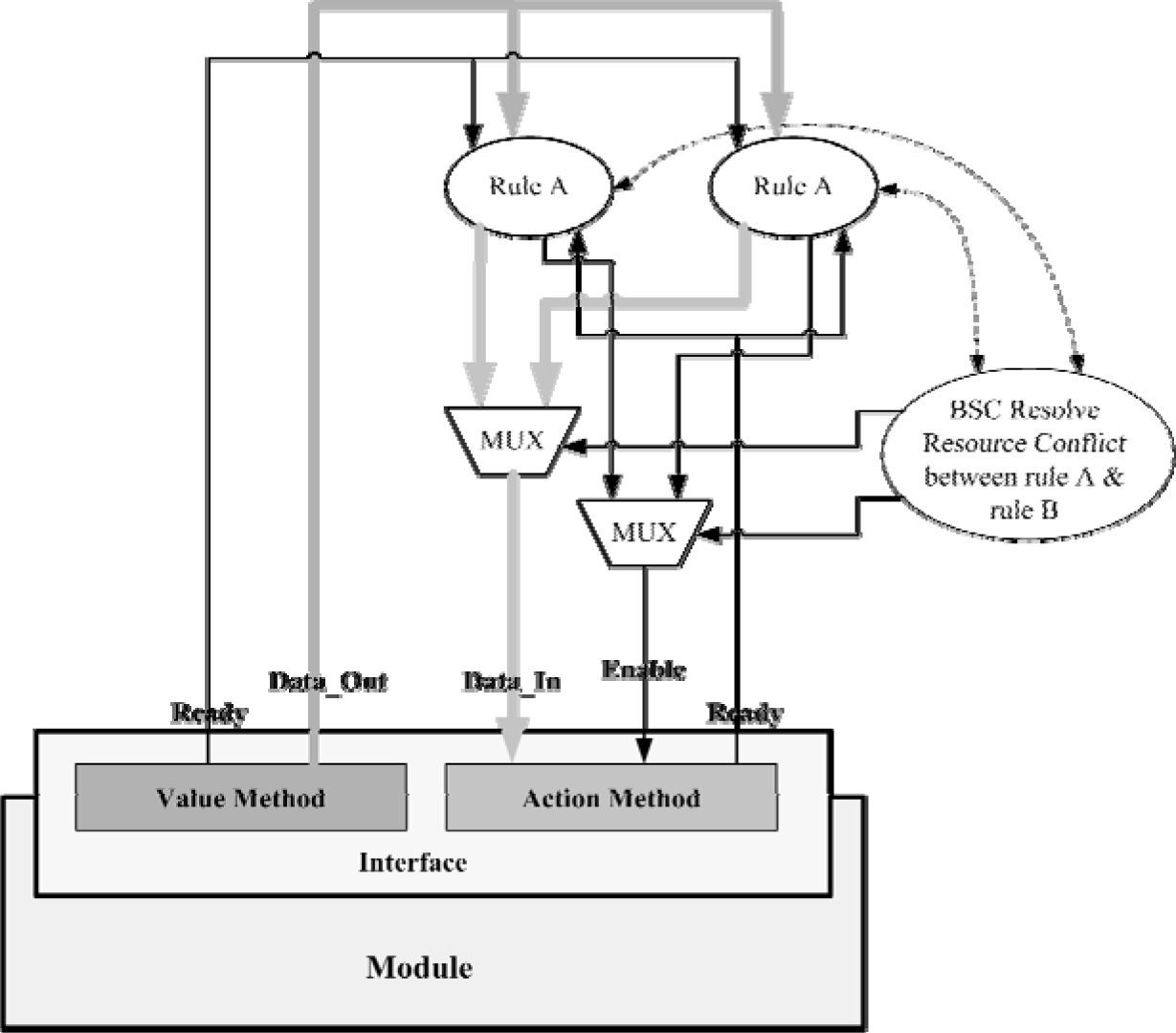
Hence the new hardware description language, Bluespec SystemVerilog (BSV) [2], is adopted to complete the above concept. Bluespec SystemVerilog, developed by MIT [4], is based on a synthesizable subset of SystemVerilog. The basic building block of BSV is Rules, instead of synchronous always blocks, can achieve correct concurrency and eliminating race condition. Each rule can be viewed as a declarative assertion expressing a potential atomic state transition. Rules need not be disjoint, i.e., two rules can read and write common state elements. The BSV Compiler (BSC) produces efficient RTL code that manages all the potential interactions between rules by inserting appropriate arbitration and scheduling logic, called handshaking circuits. The atomicity of rules can avoid unwanted race condition in large designs. Therefore BSV is suitable for designing complex algorithms by above data-oriented methodology and can generate synthesizable Verilog design quickly. The architecture of BSV module, as shown in Figure 1, includes three elements, State, Rule, and Interface, respectively. State is the storage of a module that is similar to the register and flip-flop in the digital system. Rule is the major processing circuits that can read and update the state within the module. Interface, composed by Interface Declaration and Interface Method, provide the handshaking and communication mechanism between adjacent modules. The hardware handshaking mechanisms of interface methods are shown in Figure 2. Since the orientations of interface signals can be divided into three classes: input, output, and combined input and output (inout), the proposed interface methods of BSV have three types: Action, Value, and ActionValue, respectively. In order to transfer the data at the right time, the Value (Output) interface methods consist of a Ready signal to notify the previous stage that this interface method is ready to transfer. In the Action (Input) or ActonValue (InOut) methods, it consists an Enable signal and a Ready signal to indicate that this method can be updated if the previous stage is ready to transfer.
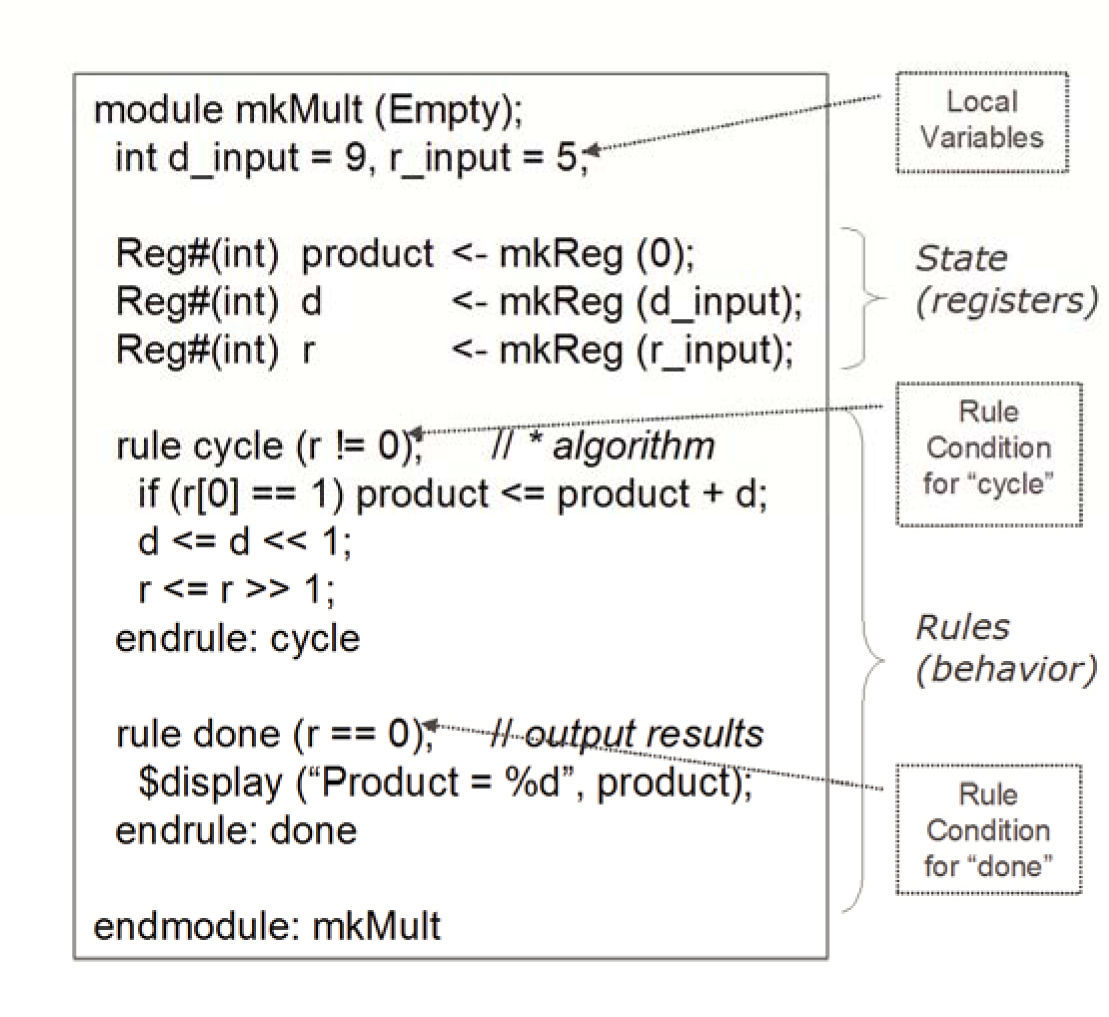
A simple sequential multiplier, composed by BSV, is proposed in Figure 3. It consists of a BSV module, local variable declaration, State declaration, and two rules. Different from conventional Verilog, the register in BSV is composed by a module and must be declared explicitly, to avoid the uncertainty register or latch. This module has two rules with mutual exclusive conditions, to avoid rule conflict. Detailed syntax of BSV please refers to [2].
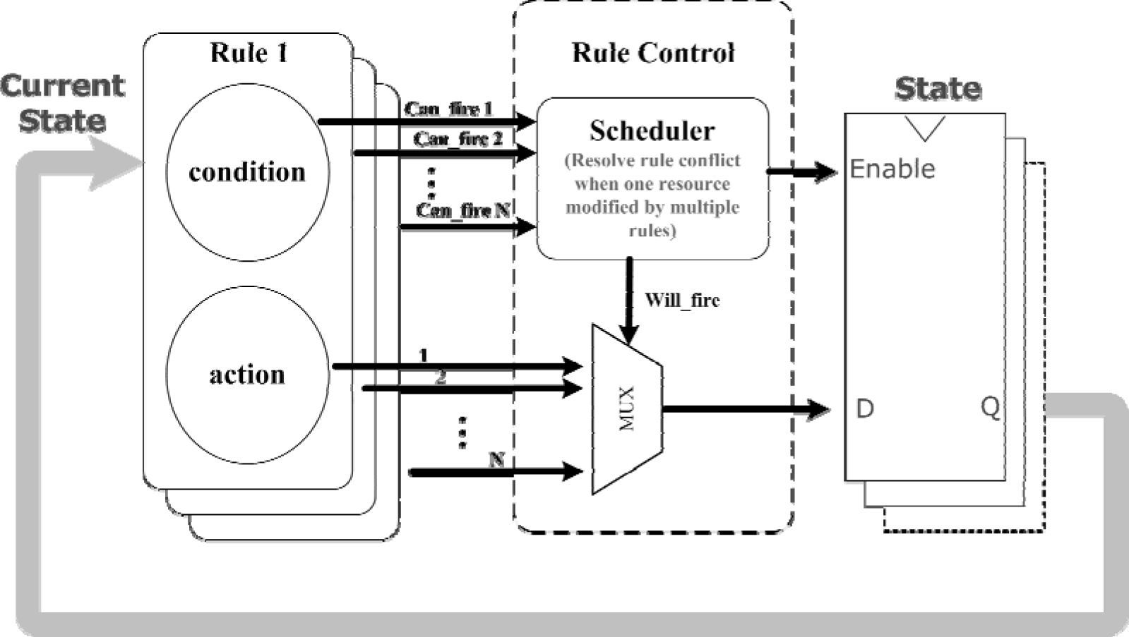
In BSV, all the hardware computations are design by rules. All rules can be executed simultaneously while the conditions are met. It is similar to Verilog always block but have the essentially difference. In the always block of Verilog, the LHS (Left-Hand-Side) needs to be reg type. In the logic synthesis stage, the reg type variables can be synthesized into flip-flop, latch, or wire according to its context. However, in BSV, the register must be explicitly declared by register module instantiation, so the designer can avoid to confusion of reg type. Without explicitly instantiation, all the variables BSV are wire which can guarantee the design without redundant flip-flops and latches. If different rules access the same resource at the same time, it will cause rule conflicts. Bluespec compiler will verify the rule conflicts, if there have unsolvable conflict, the compiler will stop compilation and return error messages. Instead of timing control of traditional ASIC design methodology, the major task of rule-based design is resolve rule-conflicts by using additional arbitrative rules. The mechanism for solving the rule conflicts and scheduling concurrent rules is shown in Figure 4. Because the rules in the BSV are composed by combinational circuits, the corresponding scheduler to solve the rule conflicts is just a simple combinational circuit. It is automatically generated by Bluespec Compiler, so there is no extra overhead for designer to maintain a precise scheduling mechanism.
4Examples of Data-Oriented Designing MethodologyIn order to verify the design facility and correctness of data-oriented methodology and realize the property that can simplify the complex design by using rule-based design, two cases are adopted to discuss the difference between data-oriented methodology and conventional timing-based methodology. The first case is the FDCT and IDCT algorithm of JPEG image compression, to illustrate the typical HDL implementation of hardware DSP algorithm. The second case is a MIPS-like CPU with five stage pipelining architecture, which can demonstrate a complex chip design consisted of a control unit and multiple functional units.
4.1Case Study 1: FDCT/IDCT algorithm of JPEG compressionThe Discrete Cosine Transform (DCT) is an important computation kernel of JPEG compression to find out the necessary information from original raw image data. The DCT method adopted in JPEG algorithm can be divided into two parts, one is Forward Discrete Cosine Transform, FDCT, the other is Inverse Discrete Cosine Transform, IDCT. The former part is used to transform space domain data to frequency domain, for accumulating the required data in the raw data stream, and then apply Huffman coding method to reduce data size. The later part is used to transform frequency domain data to space domain, which can decode JPEG image. Both of FDCT and IDCT adopt two-dimensional 8X8 matrix operations. In practical digital ASIC design, it usually adopts Row-Column decomposition to divide original two-dimensional matrix into one-dimensional to reduce hardware cost. Based on the investigation of [5], the corresponding equations of FDCT and IDCT are discussed, respectively. The equations of FDCT are listed in Eq. (1) and (2).
where
The equations of IDCT are listed in Eq. (3) and (4).
where
In this study, the above algorithms are designed by using conventional timing-control ASIC design methodology, and the proposed data-oriented ASIC design methodology. These two methodologies are implemented by Verilog and Bluespec SystemVerilog, respectively. Detailed fabrication results of above designs are discussed later.
4.2Case Study 2: MIPS-like 5-Stage Pipelined CPUIn the second case study, a classical design example, MIPS-like [6] pipelined CPU, is proposed to illustrate the design consideration of a complex digital system, which consists of a central control unit, multiple function units, multi-cycle handshaking circuits, and timing control of pipelined behaviors [7][8]. Hence it is a good example to distinguish the difference between conventional timing-control Verilog design and the proposed data-oriented Bluespec SystemVerilog design.
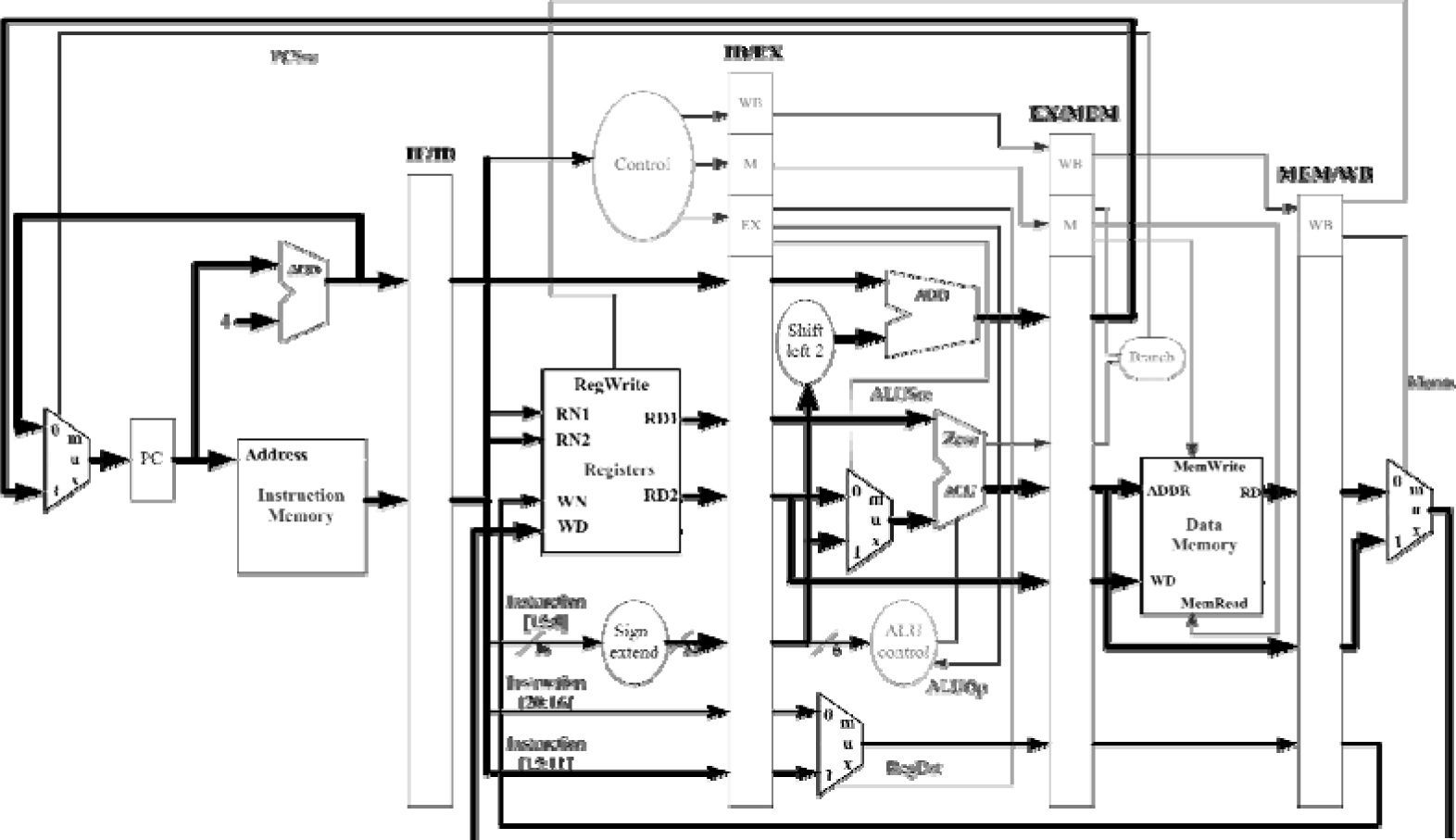
• The conventional design methodology of pipelined MIPS-like CPUFigure 5 shows the architectural datapath of MIPS-like CPU [6][8] designed by using traditional timing-control methodology. Entire CPU is divided five stages by using pipeline registers. When two or more functional units update one register concurrently, the resource conflicts are occurred. One of the solutions is to add a multiplexer to select one of them at the same time. All of the selecting signals of the multiplexers and enable signals of registers are treated as control signals, which are generated by the central control unit. All of the operations of a CPU are relied on the correct timing of control signals producing by the control unit.
The execution flow of the pipelined stage in the pipelined CPU consists of three phases. First, it reads data from current pipelined registers. Second, it operates the functionality of the assigned functional units according to the read data and control signals. Finally, it writes the operating result to the next pipelined register based on the control signals that are decoded by the control units. When the generated control signals are incorrect or issued at wrong time, the operating result is incorrect. Therefore the major challenge of conventional design methodology is to schedule the arrival time of each control signal, to implement the correct functionality of the issued instruction. This fundamental requirement of hardware design limits the design flexibility and increases the complexity of implementing new architecture.
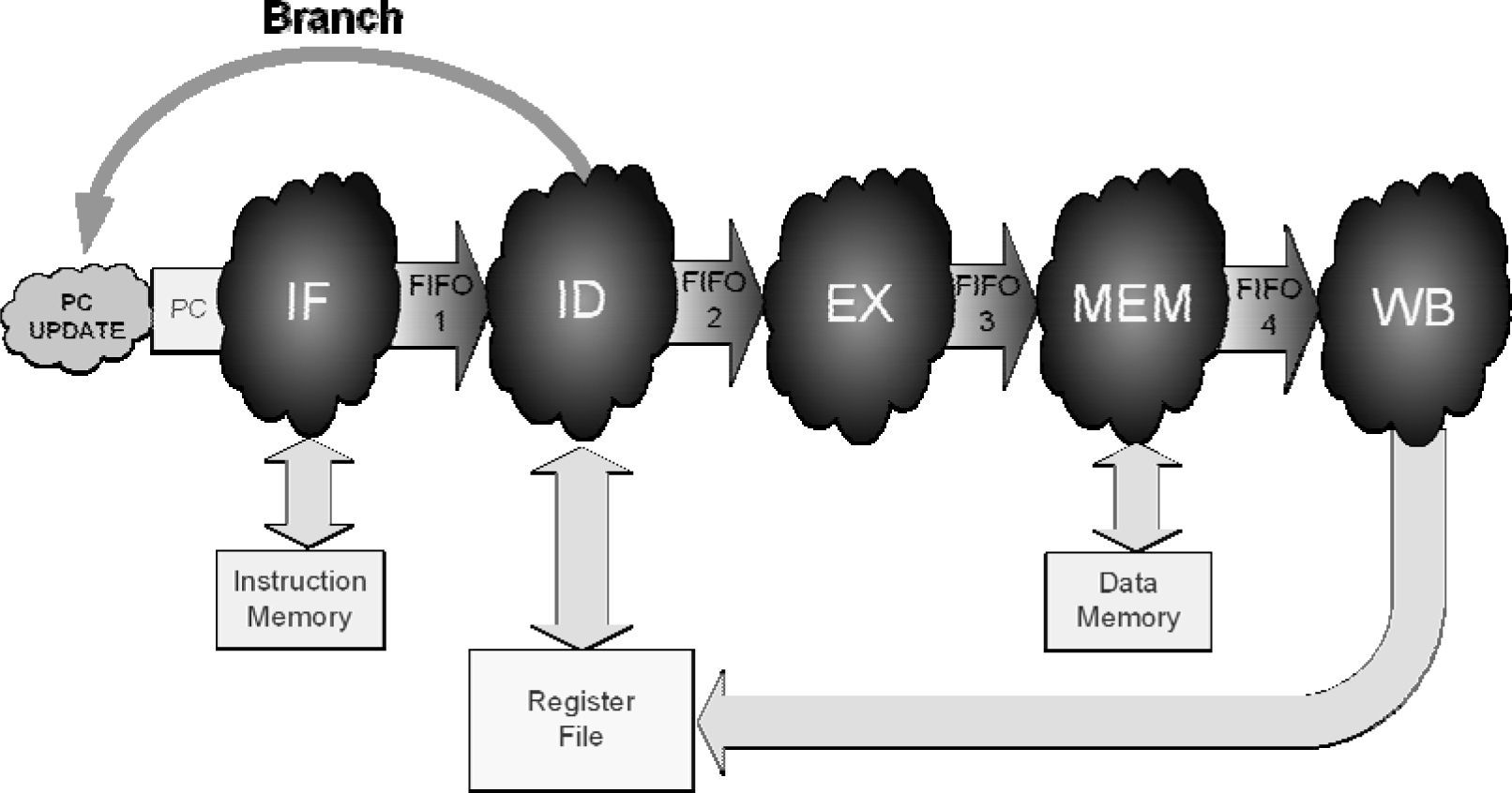
• The proposed data-oriented design methodology of pipelined MIPS-like CPUFigure 6 illustrates the datapath of the pipelined MIPS-like CPU that is designed by the proposed data-oriented methodology and Bluespec SystemVerilog (BSV). Different from conventional datapath discussed before, the new datapath is only contains several bubbles, rectangle functional blocks and FIFOs, instead of complicated functional units, control signals, and interconnection wires. The centralized control unit in conventional timing-control digital design is replaced by distributed simple handshaking circuits between two adjacent blocks that are connected by a FIFO. The detailed functional units and interconnection wires within a bubble are replace by a set of “rules”. The operations of the proposed novel datapath are described below.
Firstly, the rule of PC UPDATE is triggered every cycle to set PC by PC+4 or new branch target address. Then the rule of IF accesses the Instruction Memory block by the current PC value, fetches new instruction, and then puts the instruction into FIFO1. While FIFO1 enqueues instruction, it will trigger the rule of ID to decode new-coming instruction, and then gets operands from the Register File block. Then the resolved instruction will be pushed into FIFO2, to trigger the rule of EX. Because the blocking mechanism of the FIFO, while the FIIFO is empty or the execution condition of the rule will not match at this cycle, the rule will not be executed and pended for next cycle. It is very important for data-oriented design methodology to maintain this kind of handshaking mechanism. Therefore Bluespec SystemVerilog is adopted to implement the data-oriented methodology by using its micro protocol and atomic actions. The following rules, included EX, MEM, WB is similar to above actions.
According to above description, we can find that data-oriented design can reduce the complexity of design hardware. Instead of detailed design plan of datapaths, control signals, and timing-control mechanisms in conventional methodology, the proposed methodology can realize the hardware functionality by decision making and conflict resolving. Besides, BSV design is capable to translate into synthesizable Verilog without any modification. It can shorten the design latency of a complex SOC system.
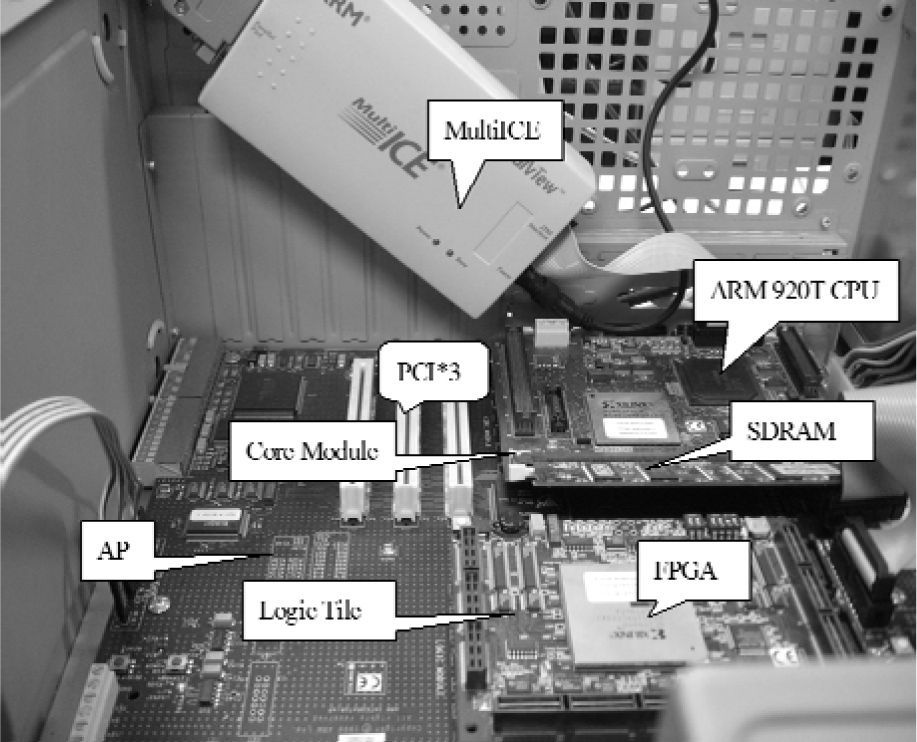
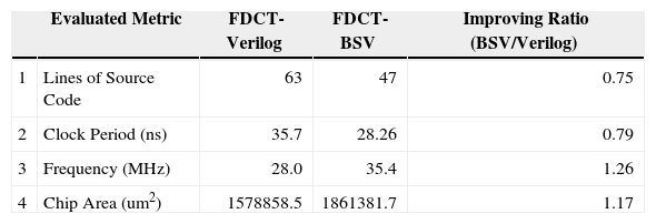
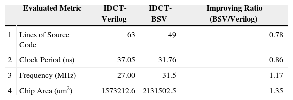
5Experimental ResultsThe functionality of proposed FDCT/IDCT and pipelined MIPS-like CPU designs have been simulated by Mentor Graphics Modelsim. These digital designs are also emulated by using ARM Integrator with Xilinx Vertex II Logic Tile [11], as shown in Figure 7. After completed the functional verification of above two case studies that demonstrates the conventional timing-control methodology (Verilog) and proposed data-oriented methodology (BSV), these six designs (FDCTVerilog, FDCT-BSV, IDCT-Verilog, IDCT-BSV, CPU-Verilog, and CPU-BSV) are synthesized by using Synopsys Design Compiler and TSMC 0.13μm technology library. Table 1 listed the difference of fabrication performance and design effort between DCT-Verilog and DCT-BSV.
Accordingly to the results listed in Table 1 and 2, the code size of FDCT-BSV/IDCT-BDV are smaller that of FDCT-Verilog/IDCT-Verilog and produce better code quality. The expected performance of chip fabrication that is generated by Synopsys Design Compiler proposed that the FDCT-BSV achieves 1.26X faster than FDCT-Verilog version. However, the chip area of FDCT-BSV is also 1.17X larger than FDCT-Verilog. Since data-oriented methodology and BSV adopt higher abstraction level modeling, the potential resource conflicts can be avoided, the design period and debug time can be shortened accordingly.
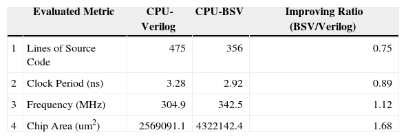
Although FDCT/IDCT is good example to illustrate the typical DSP hardware algorithm, the representative example of complex processing units in a SOC system, MIPS-like CPU, is as listed in Table 3. The datapaths of CPU-Verilog and CPU-BSV are as shown in Figure 3 and Figure 4, respectively. The code size of CPUBSV is reduced by 25 % and produced better quality, so the work frequency is improve 12%. However, the chip area is increased up to 70% due the handshaking circuits and FIFO of BSV design consumes more area. This would become the potential drawback of data-oriented methodology and BSV language.
6ConclusionsThis paper proposed a novel deign methodology, called data-oriented methodology, to overcome the design complexity of modern SoC chip, by using Bluespec SystemVerilog and the corresponding tools. The simple handshaking mechanism and blocking mechanism are adopted to make sure the correctness of adjacent blocks, the complex centralized control unit can be reduced accordingly. Two examples, FDCT/IDCT and pipelined MIPS-like CPU, are provided to compare the difference between proposed data-oriented methodology and conventional timing-control methodology. According to the proposed experimental results, the BSV version of FDCT design achieves 1.26X faster than Verilog version while it consumes 1.17X chip area. In the MIPS-like CPU example, the code size, and chip performance of BSV version is better than Verilog version by 25% and 12%, but consumes more chip area. The FPGA proven of these designs are also provided.
AcknowledgementsThis work is supported in part by the National Science Council of Republic of China, Taiwan under Grant NSC 101-2221-E-033-049.


