The use of on chip networks as interconnection media for systems implemented in FPGAs is limited by the amount of logical resources necessary to deploy the network in the target device, and the time necessary to adjust the network parameters to achieve the performance goal for the system. In this paper we present a switch architecture, with data flow control based on circuit switching and aimed for on-chip networks with a Spidergon topology, which seeks to reduce the area occupied without severely affecting the overall network performance. As a result, we obtained a switch that requires only 114 slices in its most economic version on a Virtex 4-device. We also provide a performance profile, obtained by subjecting a network formed by these switches to different synthetic workloads within a simulator. This simulator was developed as part of the design flow of the switch, and it proves to be an essential tool for the test and validation process.
El uso de redes en chip como medio de interconexión para sistemas digitales implementados en FPGA se encuentra limitado por la cantidad de recursos lógicos necesarios para implementar la infraestructura de red dentro del dispositivo, además del tiempo necesario para el ajuste de características de la red para obtener las metas de desempeño requeridas por el sistema. En este documento presentamos una arquitectura para conmutadores de red en chip, con control de flujo de datos basado en conmutación de circuitos, desarrollada con el objetivo de formar redes de topología Spidergon, y buscando reducir el área necesaria para su implementación sin castigar sobremanera el desempeño de la red. Como resultado de nuestro trabajo presentamos un conmutador que requiere solamente 114 slices de un dispositivo Virtex 4, en su versión más económica. Además proveemos de un perfil de desempeño de una red formada por nuestros conmutadores dentro de un simulador a medida. Este simulador fue desarrollado como parte del flujo de diseño del conmutador y demostró ser una herramienta esencial para la prueba y la validación del módulo.
Network on-Chip (NoC) is an emerging technology for interconnecting functional blocks in a digital system consisting of multiple processing units. The concept of NoC [1, 7, 8] has attracted interest in academia and in the development of commercial applications [9]. However, even with multiple research teams working on new developments, the NoC interconnect structures have not reached a technical maturity for emerging as the communication infrastructure that gives solution to the challenges present in modern digital systems.
A Network-on-Chip is the adaptation of the concept of computer networks applied within an integrated circuit. The network concept from computer science includes the interconnection of computers or network resources that could be mass storage units (NAS or SAN), firewalls, or dedicated servers; all of them sharing information through the network infrastructure, made of routers, switches, or bridges. The performance of a computer network is defined by its topology, the method of controlling data flow and the strategy used to guide the information through the network.
To ground these concepts in silicon, it is necessary to tailor the experience in the area of computer networks to a more restricted environment, such as an integrated circuit. In an integrated circuit, the processing elements are represented by IP blocks, general purpose processors, or memory elements.
The interconnection infrastructure can be reduced to routers or switches, given the limited area in which the digital system may extend, and the transmission medium is composed of metal lines inside the integrated circuit. The network performance is proportional to the amount of information that moves between its members and the time that the communication channels are active.
2Related WorkSome previous work in the area of on-chip networks that are worth mentioning are the following: PNOC [2], this work was develop for reconfigurable devices. PNOC implements two different kinds of network switches, one for single processing units that can communicate inside a small group of same, known as processing island, and another for a message passing between different islands. CUNOC [10] is an on-chip network with a data flow control based on package switching, because CUNOC uses a mesh topology, there must be two flavors of switches: one for the edges of the network and another for the central area. SoCWire [11] is an on-chip network developed with the objective of being compatible with the SpaceWire data transfer protocol [12]. This protocol is currently in use on missions of the European Space Agency. Star- Wheels [13], this network has a foray into the new “wheel” topology, which is very similar to Spidergon topology [4] but with the difference of implementing a “super” network switch in the center of the communication infrastructure. For a wider survey on on-chip networks, refer to [14].
3Hardware Description of the Network SwitchThe architectural design of the network switch was made keeping in mind that the module was aimed to be simple and lightweight. Because of these objectives, we needed a topology that promoted these characteristics. We chose Spidergon as the topology to be targeted because it is regular and symmetrical; these two characteristics mean that the network would look the same from any point of the net; and therefore, all the switches would be the same.
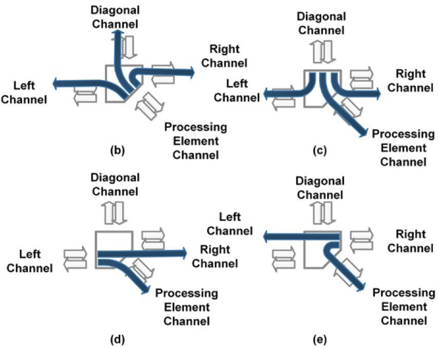
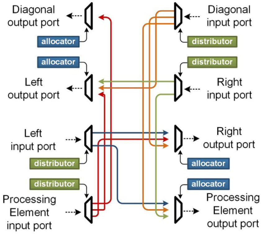
In addition, a Spidergon switch does not have a complete connection between all its communication channels, but rather it only provides links between input/output ports as shown in Figure 1. For example, the right communication channel, from a Spidergon switch, can only manage data transfers between it and the left channel and the processing unit channel. A Thorough analysis of the properties of the Spidergon topology fall outside of the scope of this document, but a comprehensive treatise can be found in [10].
Since the selected goal was the optimization of the logical resources needed to deploy one switch, a connection-oriented philosophy for controlling data flow between switches was chosen. This philosophy is known as circuit switching, and it reduces the number of storage elements needed to handle the transactions of information between switches. The reduction of storage elements takes place because, before every data transaction occurs, there must be a physical connection between the source and the destination. Once the connection is made, the data will flow as if there were a hard link between the two nodes, and temporary storage for message forwarding will not be necessary.
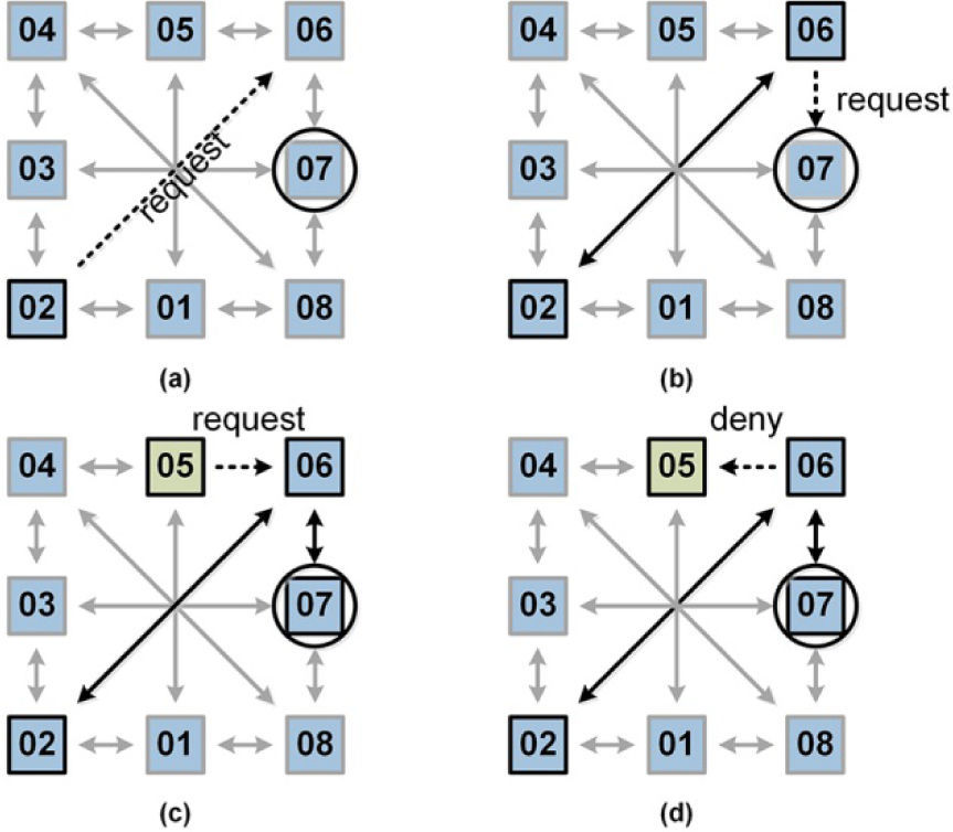
3.1Network Switch: OperationBroadly speaking, the relationship between network switches during a data transfer operation occurs as follows: Suppose the proposed network is as illustrated in Figure 2. The transaction starts when there is a need to transmit information between the nodes “02” and “07” of the network. A node is defined by a set of one switch and its processing element; however, all the communication services are provided exclusively by the switch. The path to follow to reach the destination node requires an intermediate hop on node “06”, so that node “02” sends a request for the exclusive use of the output port that connects node “06” to node “07”, as Figure 2 (a) shows.
Node number “06” shall now evaluate the petition received and determine whether the requested output port is available for assignment or not. In the case of a successful allocation by node “06”, the request sent from node “02” is transmitted transparently in the direction of the destination node, in this case node number “07”. After this operation, node “06” has already completed its arbitration tasks, hence it is limited to transmit the information received in its input port connected to node “02” to its output port connected to node “07” (This operation does not block the work of arbitration and allocation of the other ports that are not affected by communication between nodes “02” and “07”).
As opposed to the former case, the transaction flow between nodes may not be completed because some resources are not available. Our network switch is designed to handle this kind of situations as show in Figure 2 (c, d), where a data link between node “05” and node “07” is desired. In this second situation, the way to reach the destination node is by performing a jump through node “06”, which is already handling a link between node “02” and node “07”; nevertheless, the knowledge of pre-existing connections is not available for each network switch, therefore node “05” sends a request through its output port toward node “07”, and this request must make a stop in node “06”. Node “06” receives the request, but it determines that the requested port is currently in use, hence it generates a reject signal towards node “05”. After node “05” gets the reject signal, it may opt to keep the request and wait for it to be resolved satisfactorily, or it can, as in this example, momentarily withdraw its request and make another attempt after a period of time established by the processing unit.
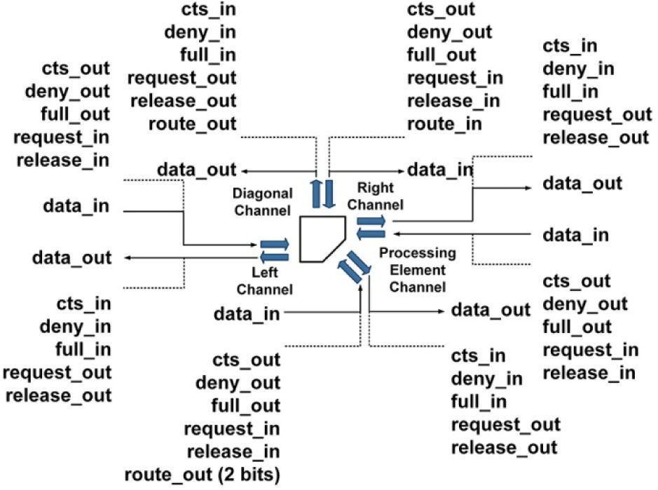
3.2Network Switch: InternalsThe switch includes four communication channels, each of which is formed by two transmission ports: a port dedicated to data logging, and a port for sending data out of the switch. At the microarchitectural level, each output port is connected to some of the input ports from the other communication channels.
The signals on each input port can be classified into control signals and data signals. The control signals are shown in Figure 3; they are used during the formation and destruction of a link between switches. During an operation of data transmission, the control signals do not have an active role on the switch. The data signals are used during the establishment of a link as carriers of the address of the destination node; after that, they serve as medium to move data packages between nodes.
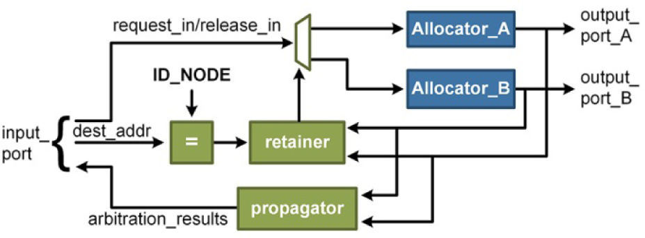
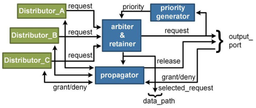
The control signals are used at three stages in the switch, these stages are responsible for implementing a policy of “decode - arbitrate - retain”. The first stage is implemented by a distributor module, shown in Figure 4, whose main task is sending all the signals entering the switch through an input port towards the correct output port, which eventually will lead the target node.
The mechanism used by the distributor to select which output port is the objective of the request is made from a comparator and a retainer; at this point, the destination address, which is carried by the data signals, is compared with the address of the current node. If the addresses are equal, it would mean that the current node is the final destination of the request, therefore, all signals are routed toward the output port of the processing element channel. Otherwise, the request will continue in the same direction from where it enters the switch, i.e., if entered by the left channel, the signal will abandon the switch through the right channel. As can be noticed, the switch does not have the ability to change the trajectory of the requests, which means simpler control logic.
The propagator module is in charge of passing the results of an arbitration process. In other words, it will let us know if a link has been successfully formed ahead or if the request has been rejected.
The next stage inside the switch is carried out by the allocator. There is an allocator per output port and its task is to choose which request will have exclusive access to the output port. As shown in Figure 5, the allocator is fed by the distributors. The arbiter-retainer module asks the priority generator which distributor will have the highest priority for the current arbitration process. The priority generator is a hardware implementation of the round-robin algorithm, meaning that the priority rotates among all entrances to the allocator, always giving lowest priority to the winner of the last resource arbitration process.
The retention stage affects both the distributor and the allocator that were involved in the last successful arbitration process. When the allocator selects a winner, the path between the distributor and the allocator, needs to be locked, so that all data arriving through the input port of the distributor may go directly to the output port of the allocator. This link must not have any meta-states while a release signal (release_in) does not arrive to the allocator.
Finally, there is the need to interconnect the distributors with their respective allocators; this connection is done by the transport logic, which consists of an arrangement of customized multiplexors and demultiplexors, designed to interact directly with the control signals from the allocators. Figure 6 shows the relationship between all the modules from the switch.
To complete all the stages inside a switch, one clock cycle is needed; for that reason, the default latency between two nodes is equal to the number of hops between them. The inverse process of tearing down a link between two nodes also takes one clock cycle per switch to be completed; however, once a switch has received the tear down signal, it is ready to establish a different link at the next clock cycle.
4Switch SimulatorAs part of the development flow of our switch, we made a network simulator. The principal role of the simulator was to provide a framework where we can test different combination of values for the switch parameters; for example, we can generate an estimate of performance for a network made of 16 switches, once we get the estimate, we can change the number of data lines between nodes and resimulate the network to know how these changes affect the performance.
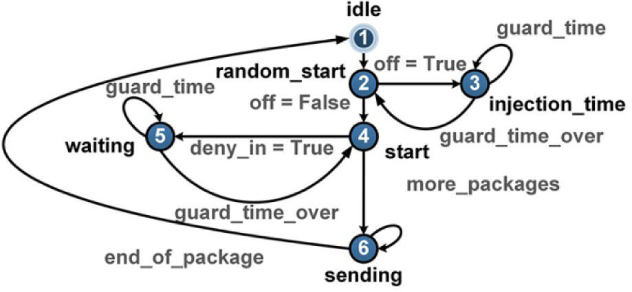
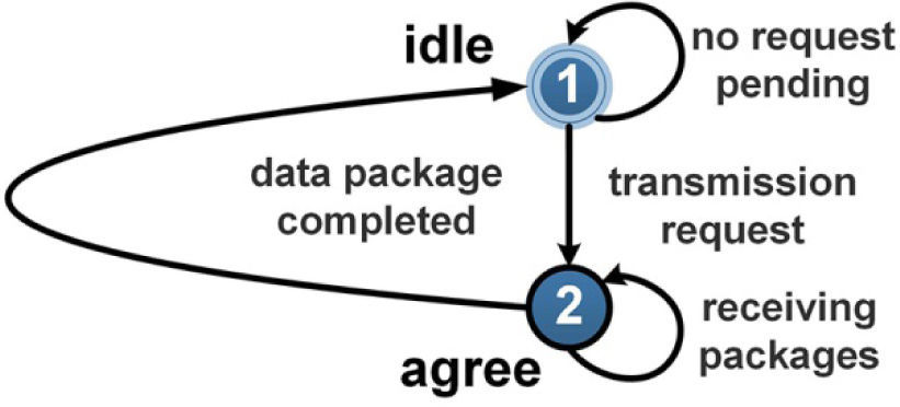
The simulator was designed under an object- oriented paradigm [5, 6]. The data infrastructure was modeled by means of 3 classes; one that represents the network switches in a true bit and cycle manner, a generator class that is responsible for imitating the operations that a processing element normally would do. The generator class is one of the most important factors in the simulator because it determines when to start a request for communication, how often the request is released, to whom the request is directed, the size of the information packages, how to set the release signal once a communication is over and handling the network contentions. This class was modeled by means of a finite state machine shown in Figure 7.
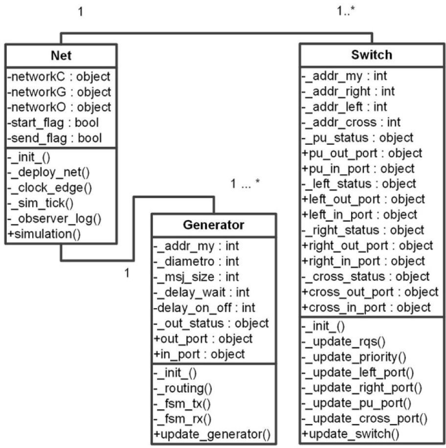
Finally, a ‘Net’ class is used as a container for all the pairs “generator - switch.” Besides a container, the net class gives orders to every element about what needs to be done to carry out the simulation, and to register all events going on in the simulated network. In Figure 8, we provide a class diagram of all the members of the simulator, as well their methods and attributes.
4.1The Switch ClassThis class describes all the behaviors and internal states from a hardware switch; for example, control and data signals are represented as boolean attributes. All the attributes are grouped by the input/output port to which they belong, and all the attributes that serve as communication points between instances of the switch class are made public.
The Switch class uses 8 methods to imitate the behavior of the hardware module, all these methods are shown in figure 8 and are used for tasks such as setting the initial values for the attributes that will be used in the simulation.
A brief description of what happens during a simulation cycle inside each switch instance is as follows: The update switch method is the interface with the other classes and is in charge of calling all the subsequent methods to complete a simulation cycle. The first task that must be done is executing the _update_rqs() method, this method works like a positive edge of a clock signal, when this method is called, all the values from the attributes representing the output ports from the neighbors switches are copied to the attributes representing the input ports of the instance that called the method; all the values obtained in this way are used by the _update_
The generator instances are paired with the switch objects to form a network node in the simulator. This class sends all the stimuli that a processing element would send to the networks switch. Broadly speaking, the generator can divide its functions in transmission and reception operations, and the transmissions going out the node are managed by the FSM shown in Figure 7. Nevertheless, it is worth noting that the routing decisions are made within the method _routing(). This method selects the traffic pattern that will be used by the node during the entire simulation. Each generator instance can select different traffic patterns by sending the correct parameters to the _routing() method. In order to add new patterns to this routine, the user must introduce the code with the new algorithm to select the valid targets nodes for communications going out of this node. A code snippet of the _routing() method is shown. if traffic == 1: while True: Self.out_port[‘addr_out’] = random.randrange / (1, self._out_status[‘total_nodos’]+1) if self.out_port[‘add_out’] != self._addr_my: break
The reception operation is limited to generate control signals to acknowledge the acceptance of incoming requests. Once a request has arrived to a generator in idle state, the finite state machine shown in Figure 9, releases the cts signal to let the source of the request know that it is clear to receive data packages. Once the number of simulation cycles necessary for the finalization of the transmission of the data have taken place, the _fsm_rx() routine, which implements the reception operations, sends a release signal to every switch object in the communication path to let them know that the transmission of data is over and the resources assigned must be deallocated.
4.3The Net ClassThe timing, for the execution of all actions needed to complete a simulation cycle, is provided by the net class. First, it receives the parameters to configure the simulation. The user provides these parameters by means of a command line interface that contains the number of nodes, number of cycles that the simulation will last, the size of packages, number of data lines between nodes, how often the nodes will release a request and the traffic pattern for each node.
Once the information is in possession of a net object, it starts to create instances of switch and generator classes. The configuration parameters for each created object are passed by the _deploy_net() method, and these parameters are used by the _init_() routines of each object for their initialization. After the simulated network has been initialized, a cyclic series of steps are executed starting with the _clock_edge() routine. This routine will trigger an update of the attributes representing the input ports of each switch object. The next step has as its goal the execution of all arbitration processes on each switch object and the evaluation of the finite state machine on every generator instance; this step is executed by the _sim_tick() routine.
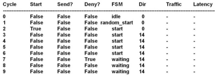
At this point, all the processes regarding the functional units of the network have been executed; hence, the final step is to register the internal state of each network switch and generator called. This action is performed by the _observer_log(). This method has access to all the internal state attributes of the generator and switch instances; thus, it will create log files as the one shown in Figure 10 for each network node on the network. All the steps above are repeated once for each simulation cycle requested by the user.
4.4Synthetic WorkloadsWorkloads are one of the most important elements in the simulations of on chip networks. The workload represents the test data to be released on the simulated network; this data represents requests for data transmissions. A workload planned too lightly can result in slanted performance profiles, showing only the best or the worse behavior of the network.
For this work, we used synthetic workloads to simulate possible scenarios in a digital system. The flexibility of the use of synthetic loads lies in the possibility of varying the traffic pattern, the addresses to which each network switch can communicate, and the frequency with which each node releases a communication request to the network. For example, a random workload will allow each node in the network to be a possible target for a communication, while a restricted workload could only allow communications to nodes numbered “05”, “03” and “07”.
5ResultsAll results presented in this paper used the next setup: the switch was implemented in a Virtex 4 - xc4vlx100-11ff1513, using the synthesis tool provided by the manufacturer. The performance results were obtained using the simulator developed specifically for this network.
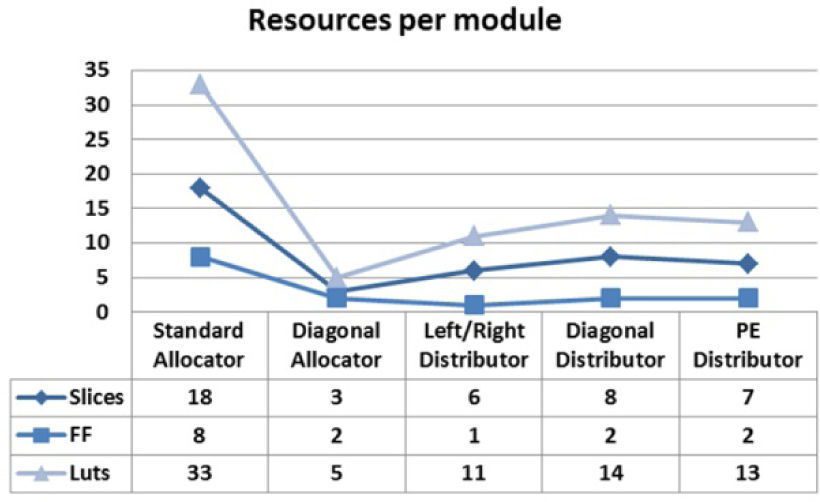
5.1Synthetic WorkloadsA detailed look at the logic resources occupied by every single internal component of the switch, as shown in Figure 11, lets us know that the critical path of combinational delays is going to be inside the allocators.
These results about occupied area should not vary in a drastic way, thanks to the decoupling between the control and data signals.
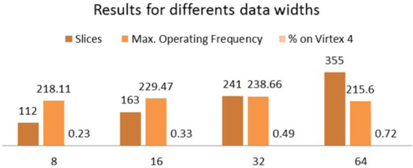
For the correct characterization of the switch performance, we synthesized 4 different switches with a different number of lines for the data transaction between them. Figure 12 shows the occupation for each switch model. It is worth noting that the increment in the width of de data lines has influence on the occupation because of the relation between the data signals and the distributors of the switch; each distributor requires us to compare the address of the destination node and its address. This operation infers a comparator with a width equal to the number of data signals, as they carry the destination address. The average percent of extra resources needed to increase the number of data lines is around 43.33% between switch models.
The most affected resources are the flip-flops from the FPGA, as they are needed in each input and output of the switch to provide a synchronous operation. It is not possible to use BRAMs because of the distributed nature of the communications channels of the switch: therefore, they are implemented using the logic element of the FPGA. As a maximum operation frequency we obtained 238.66MHz for the 32 data lines model of the switch. All other models results can be consulted in Figure 12.
5.2Simulation ResultsWe developed three scenarios with the following characteristics in common: Each network was composed of 16 nodes. We let the simulations run for 25,000 clock cycles, and the information transactions consisted of packages of 256 bytes. The results presented in this section are the average from running a single scenario ten times; this methodology was used to mitigate the presence of best/worst case for the simulation.
In particular, the first scenario interconnecting each network node, with data links of 8 bits wide, uses activation periods of between 10% and 90%. The latter refers to the probability that each node would like to start a data transaction when it is in idle, and finally the traffic pattern is random, so each node can select as a valid target all other nodes of the network. The simulator generates logs with the behavior of each node of the network. The following data are found in these logs: at which clock cycle a node generated a request, the answers to its requests, how much time it spent waiting to restart the request for a link after a reject signal, the time spent simulating an internal processing in the node, and how many cycles it was inactive.
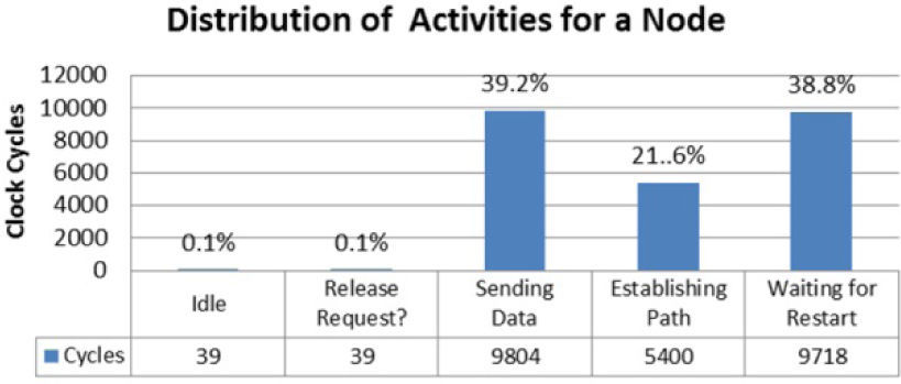
Figure 13 shows a summary of the log generated for node number 15 in one simulation from scenario 1. In particular, this node presented an activation pattern of 90%; hence, each time it was able, it requested communication with another node.
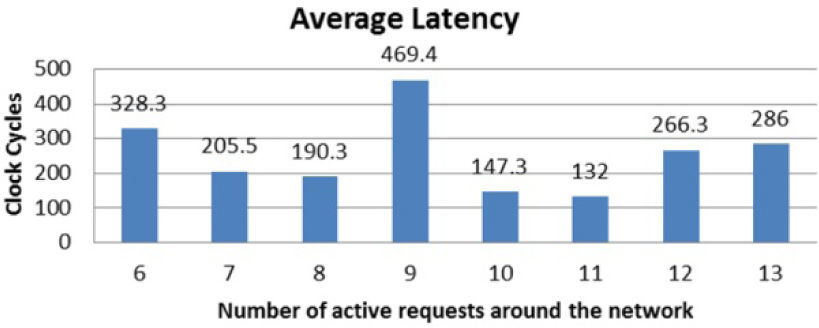
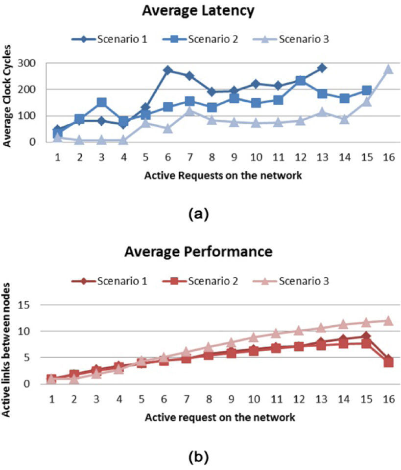
One of the most important parameters to measure in network is the latency or average time that would take to complete a satisfactory link between two nodes of the network. This parameter is highly volatile as it is affected by the current traffic on the network, for example, if just a few nodes are transmitting data then there would be a few paths occupied so there would not be the need to wait for “resource contentions”. As latency itself is not a reliable measure, we use a relation between the latency and the number of already established paths around the network. Using this relation we can evaluate the average latency of different on-chip networks, even if they use different topologies or data-flow controls. In Figure 14, we present the average latency presented in a single switch and only for 1 simulation run under scenario 2, which consists of a network formed by 16 nodes with 16-bit data links in width, activation patterns between 10% and 90%, and a random traffic pattern. As we can see, when 10 of the 16 nodes are trying to establish a connection, the network was capable of handling 9 of the connection requests satisfactorily. For global results we present the average latency of all nodes of the network from the ten runs of each scenario as shown in Figure 16 (a).
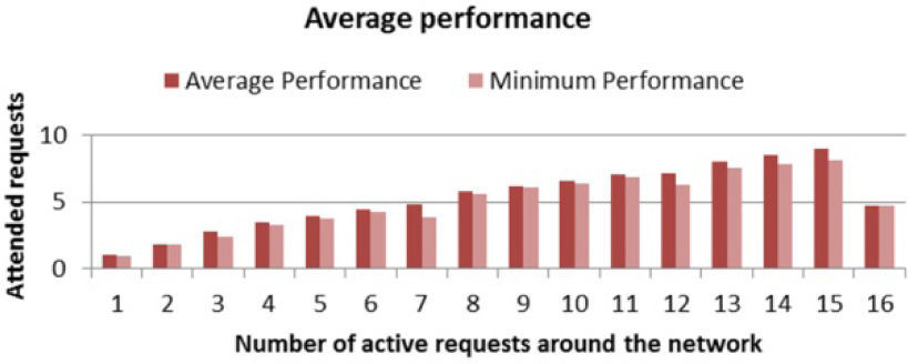
Another key parameter to evaluate a network on-chip, and therefore their switches, is the average performance, which we can think of as the number of connections between nodes that can hold the network simultaneously, in contrast with the total number of attended and unattended requests that are around the network.
For example, Figure 15 shows the average performance of one node during 10 simulations under scenario 3, which consists of a network formed by 16 nodes with 8-bit width data links, activation patterns of 100%, and a restricted traffic pattern. The performance results for the simulation of 10 runs of each scenario are presented in Figure 16 (b).
In this paper we present the description of a novel architecture for a network switch, involving a circuit switching technique, targeted to networks with a Spidergon topology. As a result, the necessary logic elements for the deployment of the network infrastructure are reduced to a minimum. In addition to the light weight architecture, the switch offers warranties once a path between 2 nodes has formed, as in-order data arrival.
It is worth noting from Figure 12 that the best balance between logic resource consumption and operation frequency is delivered by the implementation of the switch with 16-bit width data ports. In addition to the latter, this switch model can form NoCs with an ideal bandwidth of 2.29Mb/Seg in their bisection. The smallest switch of the family presents 8 lines for data transactions. This small module can find a place even on small FPGA devices. As an example of this, a network formed by 16 of these switch needs only 3.648% of the Virtex 4 device.
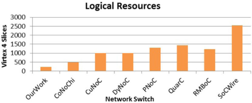
To have a better perspective of our small factor switch, Figure 17 shows a contrast between the switches proposed in: CoNoChi[15], CuNoC[10], DyNoC[16], PNoC[2], QuarC[17], RMBoC[3] and SoCWire[11]. It is easy to see that our module with 32 data lines has the lowest resource requirements; however, it is worth noting that the switches presented in the other works have added more characteristics to their design such as error handling, quality of service and reliability enhancements.
In the absence of a network simulator, the profiling of the switch performance on an on-chip network, under different stress levels, would have been a more time-consuming task because of the time needed to design hardware modules that would play the role of processing elements, and as a consequence, we would have had to use a limited number of scenarios for the profiling.
In regards to the average latency, shown in Figure 16 (a), we can notice that it remains under 300 clock cycles, even with a high number of requests around the network. However, it is worth noting that the use of a restricted traffic pattern, as in scenario number 3, improves the average latency even more than incrementing the number of data lines connecting each node with its neighbors. If the traffic pattern is previously known for a system, the right way to improve the latency will be to locate IPs with heavy communication necessities near each other; nevertheless, this is not always possible, thus the increase of the number of data lines will be an acceptable choice but with a logical resource penalty.
As for the performance, a network formed with the switches presented in this paper can handle satisfactorily up to 5 simultaneous requests; after this number, the requests start to collide into each other. This resource contention is independent from the model of the switch selected for the network. The ineffectiveness of incrementing the number of data lines is shown in Figure 16 (b) on the results between scenario 2 and scenario 3. However, the analysis of the performance for the scenario 3, which uses a restricted traffic pattern, shows that the use of smart planned traffic patterns can improve significantly the performance of the network. In this particular case the network in scenario 3 was able of handling an average of 11 requests at a maximum workload on the network.
An average from the 3 scenarios gives us an idea of what we can expect from the network under unknown circumstances; for example, we can see that the maximum performance that it can achieve is 57%, i.e., handling 9 links simultaneously between network nodes. However, if all members of the network make a simultaneous request, the performance will drop inevitably below 31.25%.
All results lead us to conclude that a network, with our switch, will provide a good solution for communications, inside on-chip digital systems with highly restricted logic elements. We also note that the simulator proved to be a valuable tool for evaluating the impact that some design options have before synthesis.
Heading: left justified, in 9-point Arial italics bold font, in sentence-case.
Content: All text must be in a two-column format. Columns are to be 8cm wide with a .59cm space between them. Also, it must be fully justified, single-spaced, in 9-point Arial regular font.


