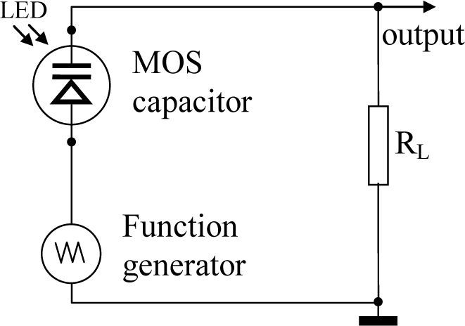
This work shows that the direct PWM output electric signal, with a duty cycle controlled by light intensity, can be obtained using a circuit containing a saw-tooth voltage generator connected in series with a dc voltage source and a metal (semitransparent gate) oxide semiconductor capacitor (MOS-C).
The internal PWM signal conversion occurs by the use of non-equilibrium physical processes in the semiconductor substrate of the MOS-C. The 10-20V amplitude limited square PWM output signal is obtained by the amplification of the sensor signal with a standard 60 dB transimpedance amplifier. The amplified output signal presents positive and negative PWM waveforms that can be easily separated using diodes. The duty of the positive part is proportional to the light intensity, whereas the negative part is inversely proportional to the intensity. The frequency operating range of this proposed instrument varies from 1 Hz to a few kilohertz. The duty cycle of the PWM output signal varies from 2% to 98% when the incident light intensity varies in the microwatts range. These new transducers or sensors could be useful for automatic control, robotic applications, dimmer systems, feedback electronic systems, and non-contact optical position sensing for nulling and centering measurements.
Cualquier sistema de instrumentación consiste de tres elementos: el sensor o dispositivo de entrada, el procesador de señales, y el receptor o dispositivo de salida. Diversos sistemas de control automático o con retroalimentación requieren una señal eléctrica de salida en forma de pulsos con modulación en su ancho (PWM). Generalmente la señal analógica de salida se transforma usando un convertidor de señal PWM.
En este trabajo se muestra que una señal de salida PWM, con una razón ancho-de-pulso/período (duty cycle) controlado por la intensidad de la iluminación, puede obtenerse directamente utilizando un circuito que contiene un capacitor metal (compuerta semitransparente)-óxido-semiconductor (MOS-C) conectado en serie con una fuente de DC y un generador de funciones que proporciona un voltaje periódico en forma de dientes de sierra.
Internamente, la conversión de señal a PWM se logra explotando los procesos físicos fuera de equilibrio que se presentan dentro del sustrato de silicio del MOS-C. La señal cuadrada PWM, cuya amplitud está limitada a 10-20V, se obtiene mediante la amplificación de la señal de transductor usando un amplificador estándar de transimpedancia de 60 dB. La señal de salida amplificada presenta una forma de onda PWM positiva y negativa que pueden separarse usando diodos.
La razón ancho-de-pulso/período de la parte positiva es proporcional a la intensidad de la iluminación, mientras que la parte negativa es inversamente proporcional a dicha intensidad. La frecuencia de operación de este instrumento se encuentra en el rango de 1 Hz hasta algunos kilohertz. La razón ancho-de-pulso/período de la señal de salida PWM varía entre 2 y 98% cuando la potencia de la iluminación es del orden de microwatts.
Este nuevo transductor o sensor podría ser útil para aplicaciones en control automático, en robótica, control de iluminación, sistemas de retroalimentación, y para la detección óptica de posición sin contacto para mediciones de centrado y anulación. Finalmente, se presenta una descripción detallada de los principios físicos y de operación de este nuevo transductor.
Among the several well-known optical sensors based on metal-semiconductor contacts or p-n junctions, metal-oxide-semiconductor capacitors (MOS-C) are known as the basic part of charge coupled devices (CCD) used in imaging technique [1].
The charging and discharging processes under irradiation in such devices are possible due to non-equilibrium processes in these semiconductor capacitors [2]. On the other hand, these processes are important for determining important physical parameters of the semiconductor substrate, such as the carrier concentration, generation and recombination times of minority carriers, and the characteristics of the semiconductor-oxide interface [3-6].
In this work we present new aspects of non-equilibrium processes in MOS capacitors with the aim of extending their optoelectronic applications as sensitive optical transducers with direct quasi-digital output in the form of a pulse-width-modulated (PWM) electrical signal. These sensors, with the new operating principle, allow for the simplification of electronic circuits necessary for automatic, robotic, and metrological applications.
We will also discuss the design and properties of a new optical position detector based on a bi-MOS structure that may be used as a sensitive null indicator with direct digital output in nulling and centering measurements.
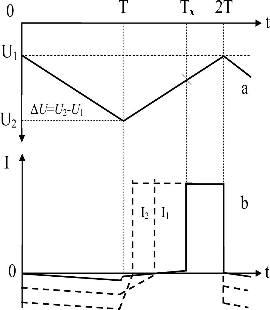
2Operating principle2.1Physical modelSensors are based on non-equilibrium physical processes that become present in MOS capacitors which are initially biased by a constant voltage in the strong inversion operating mode. If a voltage pulse is added to this dc bias, an increase of the space charge region width (SCR) to a non-equilibrium value takes place. The excess minority carriers generated in the substrate lead to a reduction of the SCR width to its initial value, and the capacitor returns to its equilibrium mode. In absence of irradiation, the retention time depends on the generation rate of minority carriers in the substrate that is determined by the generation lifetime. The irradiation effectively decreases this time in comparison to that case under dark conditions. This fact is the basis of the new optical sensors. Let us qualitatively considerate the processes occurring in the MOS capacitor, with an oxide capacitance Cox, and initially biased by a dc voltage U1 in strong inversion. At a certain time, the additional triangular voltage with amplitude U2 is applied to the gate of the capacitor as shown in Fig.1.
At the first half period, the increase of the voltage from U1 to U2, with a rate ΔU/T, leads to a time-dependent increase of the SCR width, from its stationary value Winv to its maximum W2 at t=T when a potential well is created. Both kinds of minority carriers, those generated thermally in the SCR, and those diffused from the neutral volume of the substrate, start filling this potential well, which decreases the SCR width.
If the flow of minority carriers is not too high, the potential well will not be filled completely during the first half period, and this process may also continue during the second half period until the voltage reaches Ux. At t=Tx, when the created potential well is filled, the MOS capacitor abruptly returns to its initial equilibrium state. At that time, the charge of the capacitor is Cox(Ux-U1) and the displacement current presents the constant value CoxdU/dt. The irradiation increases the generation rate of minority carriers in the substrate, and the transition time becomes shorter than that obtained under dark conditions. This is shown in Figure 1b by dashed lines for two radiation intensities.
2.2Mathematical modelUsing absolute values, the triangular voltage bias shown in Figure 1 can be described by:
The filling of the potential well with photo-generated minority carriers (the “charging” process) depends on the generation rate G. If the incident radiation has a low intensity, the charging of the MOS capacitor by the photo current occurs even when the functional voltage starts decreasing at the second half of the period.
When the potential well is filled, the reduction of the voltage till Ux at the time Tx leads to the returning of the capacitor to its initial equilibrium mode. At time Tx, the charge stored in the potential well during the photo generation is equal to the capacitor charge at the voltage (Ux-U1). This fact can be described as:
where q is the electron charge, α is the absorption coefficient of the semiconductor substrate at the wavelength of the incident radiation, and A is the gate area. The time Tx, as a function of the generation rate, can be found from (2) using the second equation of (1) for Ux:
If the MOS capacitor is connected in series with a function generator (dc plus the triangular voltage), the output signal observed in a load resistor is a pulse with a duration of 2T-Tx.
The duration of the output pulses and the duty D for the output signal (the ratio of the pulse duration to the period of the triangular voltage) are proportional to the irradiation intensity. This is because a higher intensity of the incident radiation provides a faster transition of the capacitor to its equilibrium mode. Thus, the output is a pulse width modulated electrical signal.
Taking into account (3), the equation for the output signal duty can be written as:
Taking into account that G=αPopt/Ahν, where Popt is the power of the incident optical radiation with a photon energy hν, the inverse dependence of the duty on the incident power can be written as:
The duty does not depend on the area of the capacitor. Note that in the case of a triangular voltage with period 2T, the maximum duty under irradiation can be only 0.5 when Tx is equal to the half period.
To obtain a higher range of duty due to the variation of the radiation intensity, a saw-tooth time dependent voltage must be applied to the gate. In this case, the sharp increment of the voltage from U1 to U2 during time t, which usually is 1-2% of T, creates the potential well, whereas the filling of this well by the photo generated carriers occurs during the slow decrement of the voltage from U2 to U1 during T-Δt. Then, using similar arguments as those used for the triangular voltage, the dependence of the duty on the incident radiation power is:
In this case, the duty range may vary from 0.2 to 0.9 under irradiation.
There are some frequency limitations for both, the triangular and the saw-tooth voltages cases.
The low frequency limit is determined by the generation rate of minority carriers in the SCR as well as their diffusion from the neutral substrate. The low generation rate occurs at a long generation time of minority carriers. For example, if the generation time is~0.5ms, the transition time Tx will be close to 2 s, and the low frequency limit will be 0.5 Hz. Thus, the typical operating frequency for a non-equilibrium MOS-C under illumination corresponds to a few hertz. The high frequency limit is determined by the time response of the minority carriers with respect to the voltage variation and the reactance of the capacitor, and it lies in the range of a few kilohertz.
3Results3.1Fabrication and measurements of the MOS capacitorsTo probe our conception, MOS capacitors were fabricated on high resistivity (2-4kΩ-cm) n-type silicon substrates, with a 70nm therma
lly grown oxide, and a titanium semitransparent gate. For measurements, the capacitor was connected in series with a function generator, with a dc offset and a load resistor as shown in Figure 2. The output was recorded using the digital oscilloscope TDS 3054C; a light emitting diode (LED), with emission at 0.9nm, was used to illuminate the MOS capacitors.
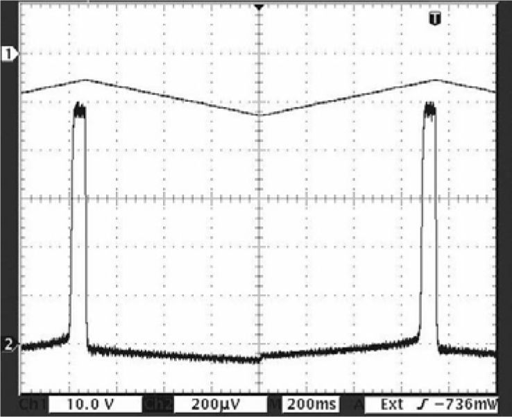
3.2Experimental results and discussionFigure 3 shows the current for the MOS capacitor under dark conditions after applying the dc and the triangular voltage. The oscillograms for the current flowing in the capacitor under illumination were recorded for an LED incident power varying in the 20nW to 0.5mW range.
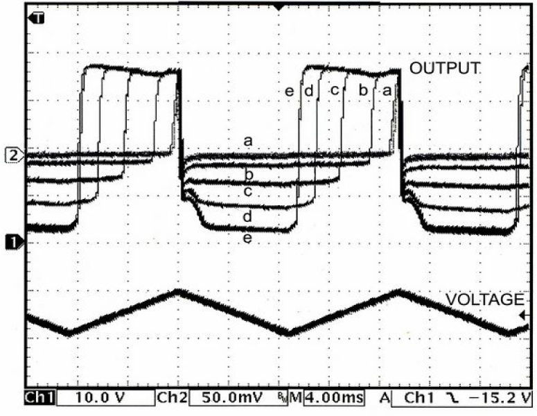
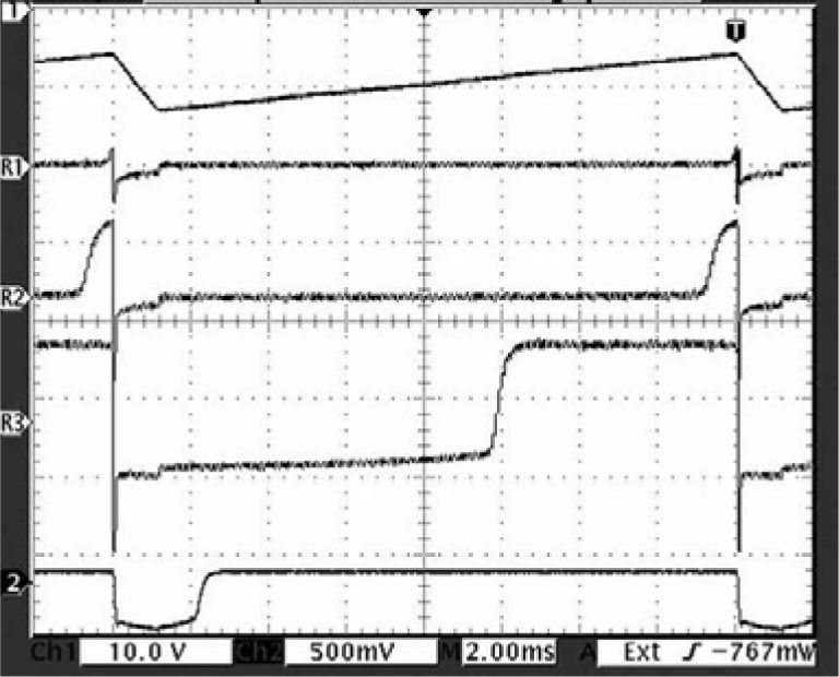
From Figure 4, one can see the difference in the transition time for the illuminated MOC-C, under different illumination conditions, when the capacitor was biased with the dc and triangular (60 Hz) voltages. The transition time decreases for an increasing illumination.
Figure 5 shows the oscillograms for the current of the illuminated MOS capacitor when a saw-tooth voltage is applied to the gate.
To obtain a “clear” PWM output signal presenting sharp transitions at both edges of the pulse, the signal from the load resistor was amplified in 103 times, and limited by the amplifier to 10V. The negative part of the signal due to the photocurrent was rejected using a diode.
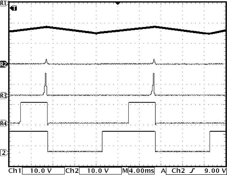
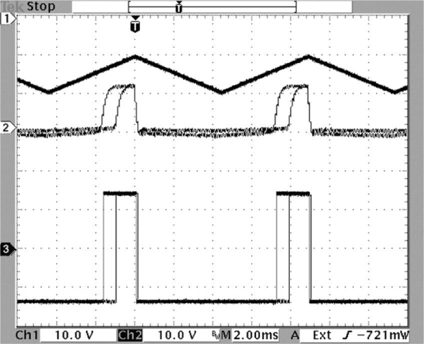
Figure 6 shows the oscillograms for the amplified output for the dc and triangular voltages applied to the gate of the MOS capacitor.
It is evident the pulse-width-modulation nature of the output signal under different illumination levels. For the case of a triangular voltage, the maximum value for the duty is 0.5.
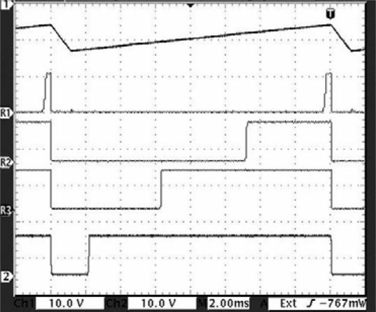
A higher range of variation for the duty, from 0.02 to 0.87, is obtained when a saw-tooth voltage is applied, as is shown in Figure 7.
From above, these non-equilibrium MOS capacitors can be used in applications such as digital sensitive optical sensors in automatic control and robotic circuits. Below, we present another new metrological application for these MOS capacitors.
3.3Bi-MOS capacitor as optical digital position sensor for nulling and centering measurements.The bicell optical detectors are well known for position sensing. They operate under the principle of having two photodiodes separated by a small gap. These elements are generally built onto a common substrate, thus their cathodes are shared. The anode or active area of each element is individually contacted. When a light spot is translated across the detector, its energy is distributed between both elements, and the difference in electrical contributions to each element defines the relative position of the light spot with respect to the center of the device. The detector provides the position information only over a linear distance of twice the spot diameter or until the edge of the spot has reached the detector gap. A linear transfer function can be obtained for a rectangular light spot because its linear movement is proportional to the percentage of its area that shifts between the elements. The sensitivity of silicon bicell position detectors is 2-3V/mm. Such detectors are most effectively used as nulling and centering devices with resolutions of 0.1micrometers or higher. Nevertheless, these devices present analog output, thus an analog-to-digital signal converter (ADC) is necessary for their application in modern circuits. Additionally, the characteristics of the ADC can affect the precision in position measurements. The use of non-equilibrium processes in MOS capacitors under illumination allows for designing new devices for position sensing.
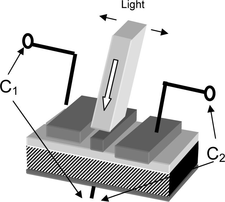
Figure 8 shows schematically the construction of our new position sensitive optical sensor. Our conception of this new position sensor is based on two MOS capacitors (C1 and C2), fabricated on the silicon substrate separated by a distance longer than the diffusion length of minority carriers in the substrate. Part of this area is covered by a metallic opaque shield. The size of the light spot must be slightly longer than the width of the shied. If the spot is located at the centre of the distance between both capacitors, approximately the same generation rate will be found at the end of each capacitor. The electric field at the lateral SCR of the biased capacitor separates the photo-generated carriers, and an equal photocurrent will flow through each capacitor. Under such conditions, and as it was shown earlier, an output PWM signal with the same duty can be recorded. A small movement of the spot will produce a misbalance in both
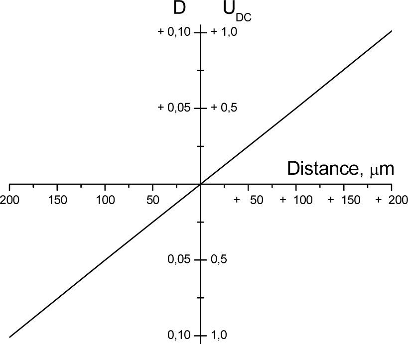
photocurrents and consequently a difference in duty for both output electric signals. If a differential amplifier is used to record these PWM signals, the information about the spot position may be obtained from the polarity and the duty of the resulting signal. Using (6), the mathematical modeling of the sensing characteristics of such position sensor has been provided for the silicon MOS capacitors, and a rectangular 2mm×1mm light spot with a power of 0.3mW/cm2 from a LED with emission wavelength at 930nm. The initial light intensity provides two equivalent PWM output signals with a duty of 0.5. Taken into account a variation of the incident optical power during the spot movement, the differential PWM signal (that can be provided by a differential amplifier) was calculated as the dependence of the resulting duty (D) on the spot position. Figure 9 shows this dependence.
The transfer function is linear for the spot movement till 200micrometers. At that limit the duty of the resulting PWM signal changes to 0.1. The polarity of the resulting PWM signal shows the direction of the movement. The use of a low-pass filter allows for transforming the 10volts output PWM signal into a dc voltage (UDC).
The slope of the dependence for UDC allows for obtaining some conclusions about the sensitivity of this new position sensor. This sensitivity is two times higher than that obtained with standard bicell silicon analog detectors. We also conducted the experimental modeling of the reported sensors fabricated on a high-resistivity silicon substrate.
The PWM output signals from both capacitors were amplified with a two-channel transimpedance amplifier. The amplified signals were added with a differential amplifier and recorded using a digital oscilloscope. Each capacitor was connected in the circuit configuration shown in Figure 2.
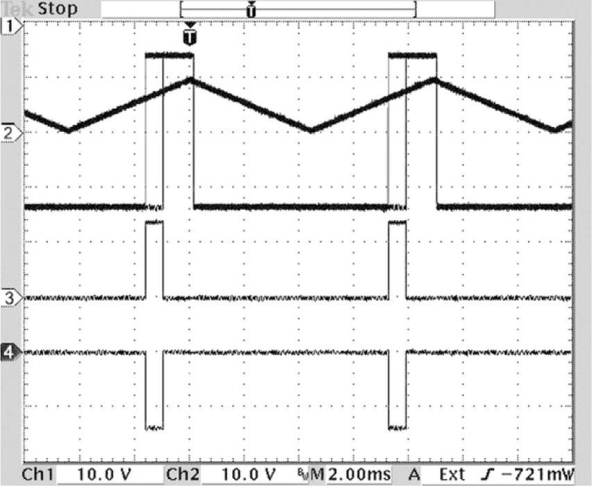
The combination of the dc 10V and the 10V triangular voltages was applied to the gates of the capacitors. The oscillograms of the output signals with and without amplification, when the dc and triangular voltages are applied to the gate of MOS capacitors, are shown in Figure 10.
Thus, the principal feature of our proposed sensor is the obtaining of a direct PWM output, with a duty that indicates the position of the light spot, whereas the polarity of the output signal indicates the direction of the spot movement.
A detailed characterization of our new sensors for nulling and centering measurements will be presented in a separate publication.
4ConclusionsIn this work we showed that non-equilibrium processes in MOS capacitors can be used for designing new optical sensors with direct pulse-width-modulated output, with a duty proportional to the light intensity. The amplified digital output using a rectangular waveform allows for the direct connection to a microcontroller or other logic circuitry. Such sensors are useful for different applications in automatic control and robotics systems because of their fabrication simplicity, as well as the possibility to simplify electronic circuits. A new type of optical sensor for nulling and centering measurements is proposed using on-chip bi-MOS capacitors. Our previous mathematical and experimental modeling showed interesting features of these sensors as a possibility to fix the position of a light spot by observing the duty value of the differential output signal, and the moving direction of the spot through through the polarity of the differential output signal.
These sensors present a linear transfer function for a light spot movement of about 200micrometers, and a two-time improved sensitivity in comparison with analog devices.
Authors thank the technicians of the Microelectronics Laboratory at the National Institute for Astrophysics, Optics and Electronics. This work was partially supported by CONACyT Mexico under grant 102397.


